3 system reaction time, 4 block diagram, System reaction time – Pilz PNOZ m EF Multi Link User Manual
Page 11: Block diagram
Function Description
Operating Manual PNOZ m EF Multi Link
1003018EN02
11
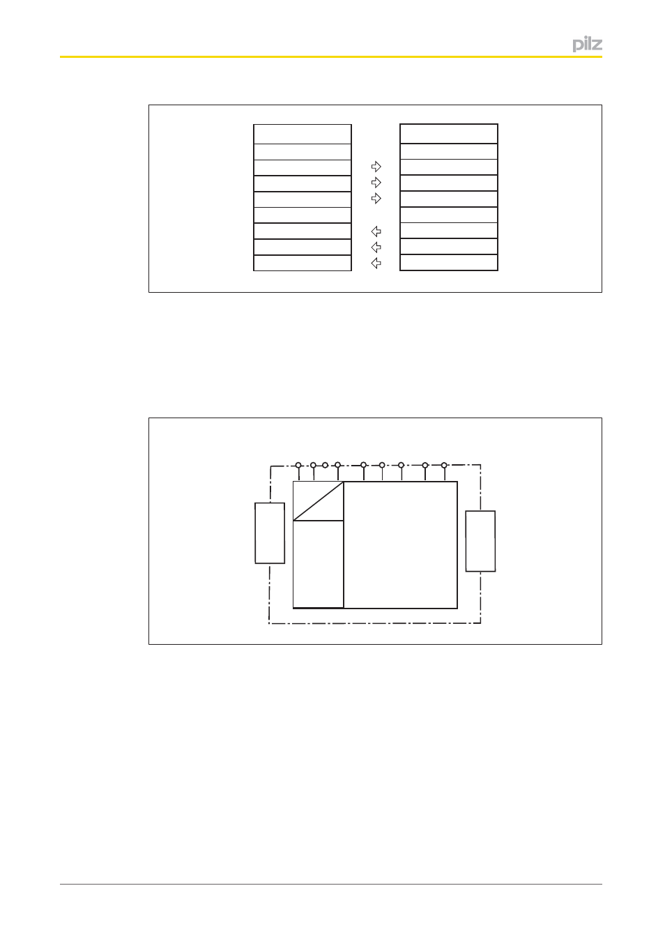
Base unit 1
Virtual outputs
o0
...
o31
Virtual inputs
i0
...
i31
Base unit 2
Virtual inputs
i0
...
i31
Virtual outputs
o0
...
o31
4.3
System reaction time
Calculation of the maximum reaction time between an input switching off and a linked out
put in the system switching off is described in the document "System Expansion".
4.4
Block diagram
Interface
to pr
evious
module
Interface
to next
module
=
Power
24V 0V n.c.FE
=
CB- CGround
CA- CB+
CA+
See also other documents in the category Pilz Sensors:
- PSEN in1p (16 pages)
- PSEN in1n (12 pages)
- PSEN rs2.0-300 (16 pages)
- PSEN rs1.0-175 (16 pages)
- PSEN enc m1 eCAM (46 pages)
- PSENme 1S / 1AS (16 pages)
- PSENme 1S / 1AS (6 pages)
- PSENme 2 / 2A (6 pages)
- PSENme 4 / 4A (5 pages)
- PNOZ m EF 2MM (6 pages)
- PSEN 1.1b-23/PSEN1.1-20/8mm/10m/EX/1unit (8 pages)
- PNOZ m EF 2MM (8 pages)
- PSEN 1.1p-20/PSEN 1.1-20/8mm/ 1unit (6 pages)
- PSEN 1.1p-29/PSEN 1.1-20/7mm/ix1/ 1unit (6 pages)
- PSEN 1.1b-25/PSEN1.1-20/8mm/10m/EX/1unit (8 pages)
- PSEN 1.1p-22/PSEN 1.1-20/8mm/ix1/ 1unit (6 pages)
- PSEN 1.1-10 / 1 actuator (6 pages)
- PSEN 1.2p-20/PSEN 1.2-20/8mm/ 1unit (6 pages)
- PSEN 1.1p-23/PSEN 1.1-20/8mm/ATEX/ 1unit (8 pages)
- PNOZ m EF 2MM (6 pages)
- PSEN 1.2p-22/PSEN 1.2-20/8mm/ix1/ 1unit (6 pages)
- PSEN 1.1p-25/PSEN 1.1-20/8mm/ATEX/ix1 (8 pages)
- PSEN 1.1-10 / 1 actuator (6 pages)
- PSEN 1.2p-23/PSEN 1.2-20/8mm/ATEX/ 1unit (8 pages)
- PSEN 1.1a-20/PSEN 1.1-20 /8mm/5m/1unit (6 pages)
- PSEN 1.2p-25/PSEN 1.2-20/8mm/ATEX/ix1 (8 pages)
- PSEN 1.1a-22/PSEN 1.1-20 /8mm/5m/ix1/1un (6 pages)
- PNOZ m EF 2MM (6 pages)
- PSEN ma1.3a-20/PSEN ma1.3-08/8mm/1unit (10 pages)
- PSEN ma1.3a-22/PSEN ma1.3-08/8mm/1unit (10 pages)
- PSEN ma1.3b-23/PSEN ma1.3-08/8mm/1unit (10 pages)
- PSEN ma1.3b-25/PSEN ma1.3-08/8mm/1unit (10 pages)
- PSEN ma1.3p-20/PSEN ma1.3-08/8mm/1unit (10 pages)
- PSEN ma1.3p-22/PSEN ma1.3-08/8mm/ix1/1un (10 pages)
- PSEN ma1.3n-20/PSEN ma1.3-08/8mm/1unit (12 pages)
- PSEN ma1.3-20 M12/8-0.15m 1switch (10 pages)
- PSEN ma1.4p-52/PSEN ma1.4-03mm/ 1unit (10 pages)
- PSEN ma1.4p-51/PSEN ma1.4-03mm/ 1unit (10 pages)
- PSEN ma1.4n-51/ 1switch (9 pages)
- PSEN ma1.4n-50/PSEN ma1.4-03mm/ 1unit (10 pages)
- PSEN ma1.4-51 M12/8-0.15m 1switch (10 pages)
- PSEN ma1.4p-57/PSEN ma1.4-10mm/ 1unit (10 pages)
- PSEN ma1.4a-52/PSEN ma1.4-03mm/ 1unit (10 pages)
- PSEN ma1.4a-51/PSEN ma1.4-10mm/ 1unit (10 pages)
- PSEN ma1.4p-50/PSEN ma1.4-03mm/ 1unit (10 pages)