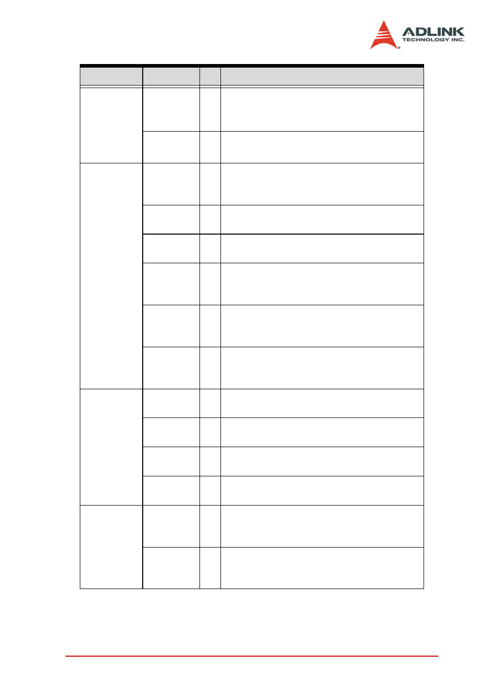
Table 3-6: pcie-7350 afi signal description – ADLINK PCIe-7350 User Manual
Page 67
Function Block and Operation Theory
57
Function
Signal
I/O
Description
I
2
C Master
SCL
O
I
2
C Clock
– I
2
C clock signal to slave
device capable of clock rate up to
1953.125KHz.
SDA
I/O
I
2
C Serial Data
– Data signal for I
2
C read/
write communication.
SPI Master
SCK
O
SPI Clock
– SPI clock signal to slave
device capable of clock rate up to
62.5MHz.
SDI
I
Master Input Slave Output
– Data signal
for SPI read communication.
SDO
O
Master Output Slave Input
– Data signal
for SPI write communication.
CS_0
O
Chip Select of Slave Device 0
– Output
signal to select the desired SPI slave
device 0.
CS_1
O
Chip Select of Slave Device 1
– Output
signal to select the desired SPI slave
device 1.
CS_2
O
Chip Select of Slave Device 2
– Output
signal to select the desired SPI slave
device 2.
External
Trigger in
DI-Start
I
DI Start Trigger in
– External digital trigger
signal to begin an acquisition operation.
DO-Start
I
DO Start Trigger in
– External digital trig-
ger signal to begin a generation operation.
DI-Pause
I
DI Gate Trigger in
– External digital signal
to start/pause an acquisition operation.
DO-Pause
I
DO Gate Trigger in
– External digital sig-
nal to start/pause a generation operation.
Trigger out
DI_SW
O
DI Trigger out
– A pulse signal output gen-
erated by PCIe-7350 when receiving a
software start command of DI.
DO_SW
O
DO Trigger out
– A pulse signal output
generated by PCIe-7350 when receiving a
software start command of DO.
Table 3-6: PCIe-7350 AFI Signal Description