ADLINK PCIe-7350 User Manual
Page 14
4
Introduction
If you want to have DO throughput to be up to 200M Byte/s, the
data size is limited to less than the 8K FIFO size by the following
steps:
Step1:
Read 8K DO data from system memory into DO FIFO
by DMA before writing 8K DO data from DO FIFO to
the external device
Step2: After 8K DO data are all stored into DO FIFO, and
then start writing these 8K DO data to the external
device with 50MHz DO sample clock rate and 32-bit
data width.
External clock rate can be up to 100 MHz, but only support 8 or
16-bit data width because the DI data throughput can’t exceed 200
MB/s
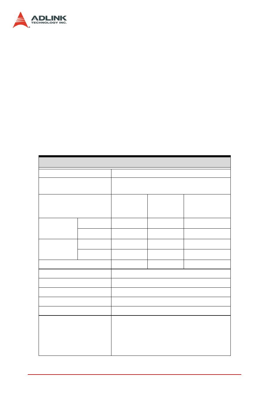
Application Function I/O (AFI)
Number of channels
8
Direction
(programmable)
Input or output,
per channel basis
Logic Levels
(programmable)
1.8 V
2.5 V
3.3 V
(5 V Compati-
ble)
Input
Voltage
Min. V
IH
1.2 V
1.6 V
2 V
Max. V
IL
0.63 V
0.7 V
0.8 V
Output
Voltage
Min. V
OH
1.6 V
2.3 V
3.1 V
Max. V
OL
0.2 V
0.2 V
0.2 V
Driving capacity (max.)
±8 mA
±16 mA
±32 mA
Input impedance
10 KΩ
Input protection range
-1 to 6 V
Output impedance
50 Ω
Power-up initial state
Tri-State / All digital inputs
Output protection range
-0.5V to 3.8V
Supported Mode
(programmable)
I
2
C master
SPI master
Handshaking
External trigger in/out
DI/DO sample clock in/out