2 programmable logic level, Programmable logic level, Table 3-1: pcie-7350 logic levels – ADLINK PCIe-7350 User Manual
Page 31
Function Block and Operation Theory
21
3.2
Programmable Logic Level
To interface different logic level applications, the PCIe-7350 sup-
ports three software selectable logic levels of 1.8 V, 2.5 V, or 3.3 V
(5 V compatible) for all digital I/O lines, sample clocks, I
2
C, SPI,
triggers, and events. When you choose one of these three logic
levels, all the I/O lines will be at the same logic level you choose.
Below are the definition and high/low range for different logic lev-
els. When connecting PCIe-7350 to a device under test (DUT),
you must ensure that the interface voltage levels are compatible.
V
IH
: The digital input voltage at logic high; senses a binary
one (1)
V
IL
: The digital input voltage at logic low; senses a binary
zero (0)
V
OH
: The digital output voltage at logic high; generates a
binary one (1)
V
OL
: The digital output voltage at logic low; generate a
binary zero (0)
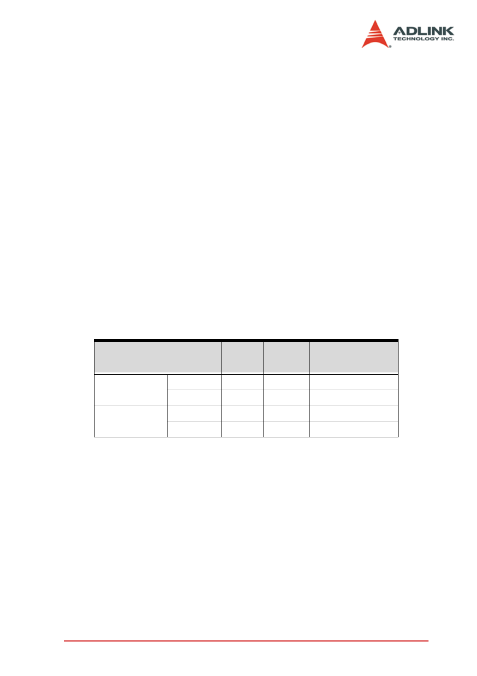
Logic Levels
1.8 V
2.5 V
3.3 V
(5 V compatible)
Digital Input
Min. VIH
1.2 V
1.6 V
2 V
Max. VIL
0.63 V
0.7 V
0.8 V
Digital Output
Min. VOH
1.6 V
2.3 V
3.1 V
Max. VOL
0.2 V
0.2 V
0.2 V
Table 3-1: PCIe-7350 Logic Levels