3 specifications, Specifications, 2introduction – ADLINK PCIe-7350 User Manual
Page 12
2
Introduction
1.3
Specifications
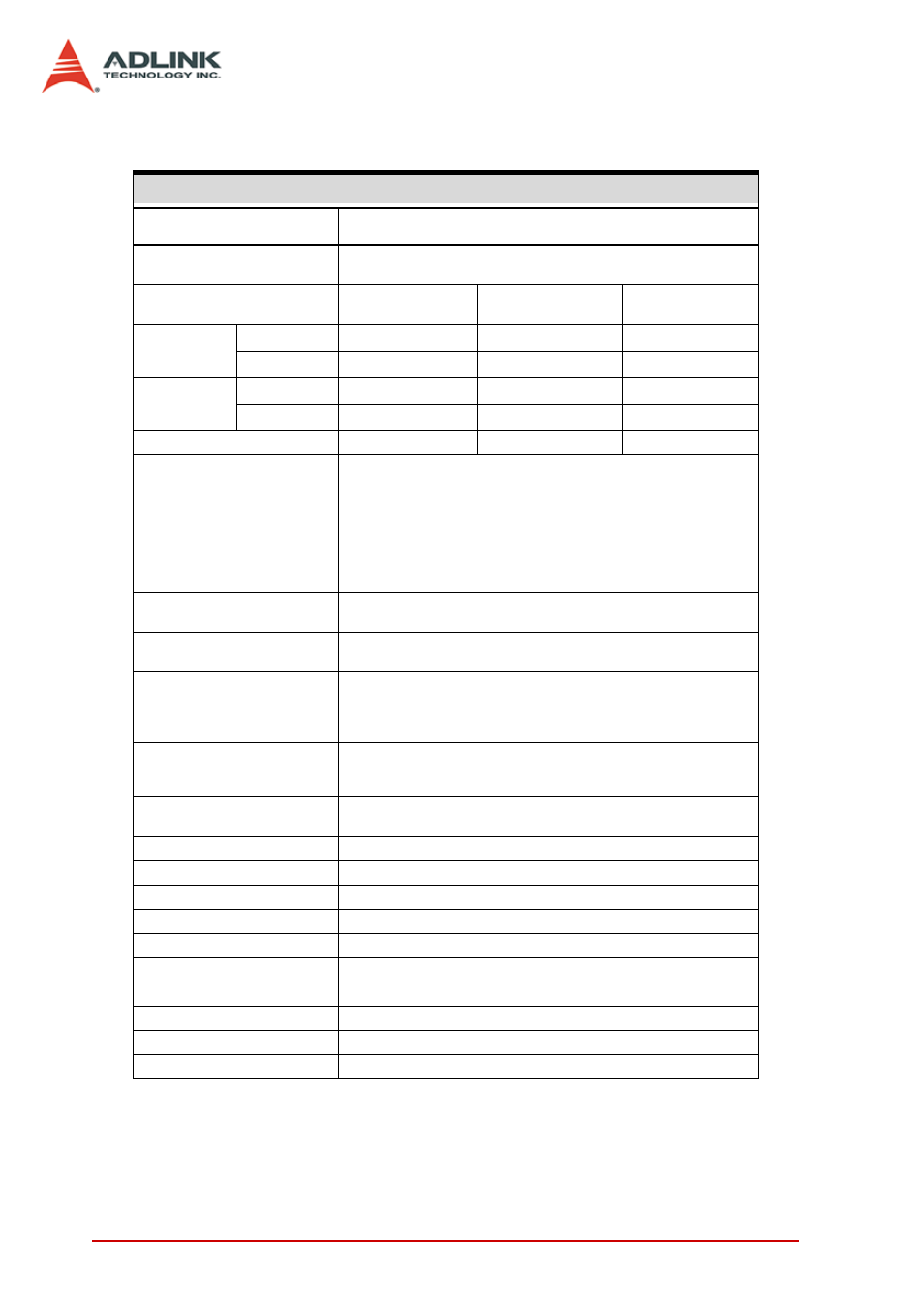
Digital I/O Specifications
Number of
Channels
32
Direction
(programmable)
Input or output,
per group (8 channel) basis
Logic Level
(programmable)
1.8 V
2.5 V
3.3 V
(5 V compatible)
Input
Voltage
Min. V
IH
1.2 V
1.6 V
2 V
Max. V
IL
0.63 V
0.7 V
0.8 V
Output
Voltage
Min. V
OH
1.6 V
2.3 V
3.1 V
Max. V
OL
0.2 V
0.2 V
0.2 V
Driving capacity(max.)
±8 mA
±16 mA
±32 mA
Throughput
Digital Input:
Maximum: 200 MByte/s (32-bits input @ 50 MHz) (data size≤250k
samples)
Sustained: 192 MByte/s (data size>250k samples) (Note* )
Digital Output:
Maximum: 200 MByte/s (32-bit output @ 50 MHz) (FIFO load mode,
max. 8k samples)
Sustained: 119.2 MByte/s (Note**)
FIFO Size
Digital Input: 8k samples
Digital Output: 8k samples
Data Transfer
Software Polling
Bus-mastering DMA with Scatter-Gather
Clocking Modes
Internal clock: max. 50 MHz
External clock: max. 100 MHz
Handshaking
Burst handshaking
Trigger Source
Software
External Digital signal
Pattern match
Trigger Modes
Post trigger with re-trigger
Gate trigger
Input impedance
10 KΩ
Input protection range
-1 to 6 V
Output impedance
50 Ω
Power-up initial state
Tri-State / All digital inputs
Output protection range
-0.5 V to 3.8 V
Dimensions
168 mm x 112 mm (not including connectors)
Connectors
68-pin VHDCI female x1 SMB x2
Operating Temp.
0 to 55° C
Storage Temp.
-20 to 70° C
Relative Humidity
5 to 95%, non-condensing