14 hardware information, Table 2-2: i/o signal descriptions, Table 2-3: smb jack connector signal descriptions – ADLINK PCIe-7350 User Manual
Page 24
14
Hardware
Information
Signal Descriptions
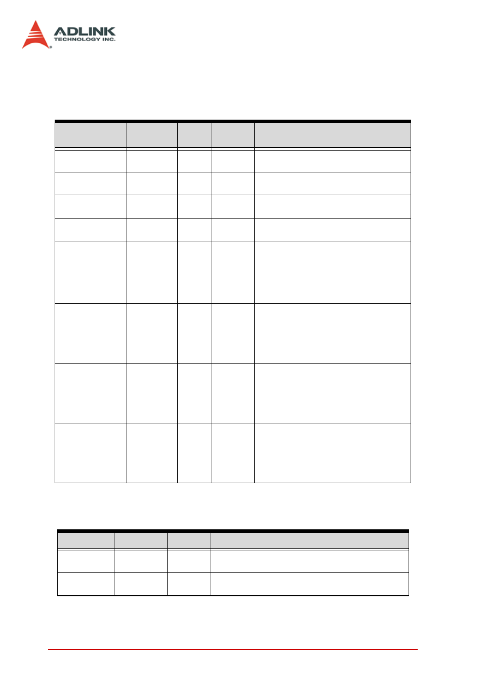
Below are the signal descriptions for the SCSI-VHDCI and SMB
connectors:
SMB Jack Connector Signal Description
Pin
Number
Signal
Name
Signal
Type
Direction Description
25, 27, 29, 31, 59,
61, 63, 65
D0 – D7
Data
I/O
Port_A bi-directional digital data lines
17, 19, 21, 23, 51,
53, 55, 57
D8 – D15
Data
I/O
Port_B bi-directional digital data lines
9, 11, 13, 15, 43,
45, 47, 49
D16 – D23
Data
I/O
Port_C bi-directional digital data lines
1, 3, 5, 7, 35, 37,
39, 41
D24 – D31
Data
I/O
Port_D bi-directional digital data lines
8, 26, 30, 52, 60,
64
AFI0 – AFI5
Control
/Data
I/O
Application Function I/O, can be config-
ured as the following control signals:
I
2
C/ SPI
Handshaking signal
External trigger in/out
Event out
33
AFI6
Control
/Data
I/O
Application Function I/O, can be config-
ured as the following control signals:
Handshaking signal
External trigger in/out
Event out
DO sampled clock in/out
67
AFI7
Control
/Data
I/O
Application Function I/O, can be config-
ured as the following control signals:
Handshaking signal
External trigger in/out
Event out
DI sampled clock in/out
2, 4,6, 10, 12, 14,
16, 18,20, 22, 24,
28, 32, 34, 36, 38,
40, 42, 44, 46, 48,
50, 54, 56, 58, 62,
66, 68
GND
Ground
--------
Ground reference for Data I/O and AFI I/O
Table 2-2: I/O Signal Descriptions
Signal Name
Signal Type
Direction
Description
CLK IN
Clock
I
External clock input for DI/DO sampled clock from
external device to the PCIe-7350
CLK OUT
Clock
O
DI/DO sampled clock exporting from the PCIe-7350 to
an external device
Table 2-3: SMB Jack Connector Signal Descriptions