Introduction 5, Timing specifications, Timing accuracy – ADLINK PCIe-7350 User Manual
Page 15
Introduction
5
When you enable phase shift, the clock must be continuous and
free-running
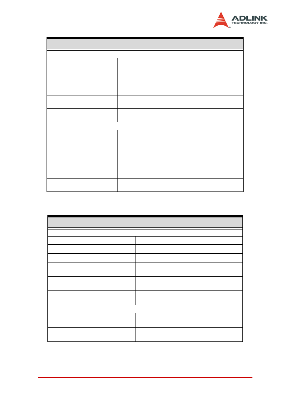
Timing Specifications
Sample Clock
Clock Sources
Internal clock: on-board 100MHz with 16-bit divider
External clock:
1. AFI6 (for DO)
2. AFI7 (for DI)
3. SMB CLK in
Internal Clock Rate
(programmable)
1526 Hz – 50 MHz
(100 MHz/ N; 2≤N≤65,535)
Ext. frequency range
0 - 100 MHz (no phase shift)
2 MHz - 50MHz (phase shift enabled)*
Phase shift
Internal clock: N/A
External clock: 16 steps; 1 step = 22.5°
Sample Clock Exporting
Destination
1. AFI6 (only for DO)
2. AFI7 (only for DI)
3. SMB CLK out
Frequency range
0 ~ 50 MHz (no phase shift)
2 MHz ~ 50MHz (phase shift enabled) (note3)
Clock jitter
Period jitter: 160 ps
Clock duty cycle
50%
Phase shift resolution
1/16 of external sampled clock period
(16 steps; 1 step = 22.5°)
Timing Accuracy
Acquisition Timing
Channel-to-Channel skew
±1.08 ns
Setup time to sampled clock (t
SU
)
2 ns
Hold time to sampled clock (t
H
)
2 ns
Time delay of external sampled clock
from AFI7 to internal (t
AF7D
)
7.22 ns
Time delay of external sampled clock
from SMB CLK in to internal (t
SMBID
)
8.02 ns
Time delay of DI data from VHDCI
connector to internal (t
DID
)
3.26 ns - 4.34 ns
Generation Timing
Exported Clock SkewAFI6 -to- SMB
CLK out(t
ECskew
)
3.24 ns
Exported Clock (AFI6) -to- DO Data
Delay (t
AF62D
)
600 ps - 5 ns