4 phase shift of sample clock, Phase shift of sample clock, Figure 3-6: phase shift of sample clock – ADLINK PCIe-7350 User Manual
Page 37: Pcie-7350 card, Function block and operation theory 27
Function Block and Operation Theory
27
3.4
Phase Shift of Sample Clock
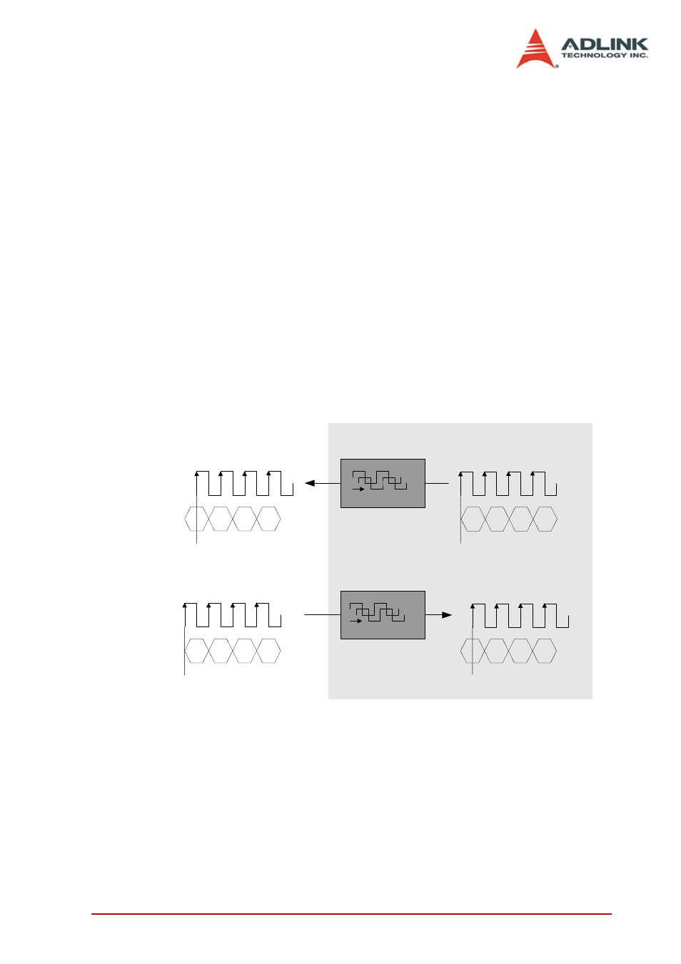
PCIe-7350 features phase shift of sample clock (on SMB connec-
tor or AFI6 & AFI7 of SCSI-VHDCI connector). The sample clock
can be from external DUT or can be the exporting clock generated
from internal time base. The resolution of phase shift is 4-bit (16
steps) implemented by Phase-Locked Loop (PLL) function of
FPGA. In other words, the phase shift of sample clock is 22.5° x N,
where N is any integer from 1 to 15. Furthermore, in phase shifting
mode, the supported clock frequency is from 2 MHz to 50 MHz.
This function can optimize the timing of digital pattern acquisition
or generation to avoid sampling/exporting the data from/to DUT at
transition state. Therefore, for digital input, the data can be sam-
pled in clean and valid timing instead of transition timing. For digi-
tal output, it can fine tune the exporting clock to avoid the sampling
of DUT at setup time or hold time instead of aligning the data.
Figure 3-6: Phase Shift of Sample Clock
Acquisition of Digital Data
External
sampled clock
(from DUT)
DI Data
(from DUT)
Generation of Digital Data
Exported
sampled clock
(to DUT)
DO Data
(to DUT)
D0
D1
D2
D3
D0
D1
D2
D3
D0
D1
D2
D3
D0
D1
D2
D3
16 steps phase shift
16 steps phase shift
PCIe-7350 Card
Valid area
Transition area
Valid area
Transition area