Adept system – Digilent 410-182P-KIT User Manual
Page 4
Nexys3 Reference Manual
Doc: 502-182
page 4 of 22
Adept System
Digilent's Adept high-speed USB2 system can be used to program the FPGA and PCM devices, run
automated board tests, add PC-based virtual I/O devices (like buttons, switches, and LEDs) to FPGA
designs, and exchange register-based and file-based data with the FPGA. Adept automatically
recognizes the Nexys3 board and presents a graphical interface with tabs for each of these
applications. Adept also includes public APIs/DLLs so that users can write applications to exchange
data with the Nexys3 board at up to 38Mbytes/sec. The Adept application, an SDK, and reference
materials are freely downloadable from the Digilent website.
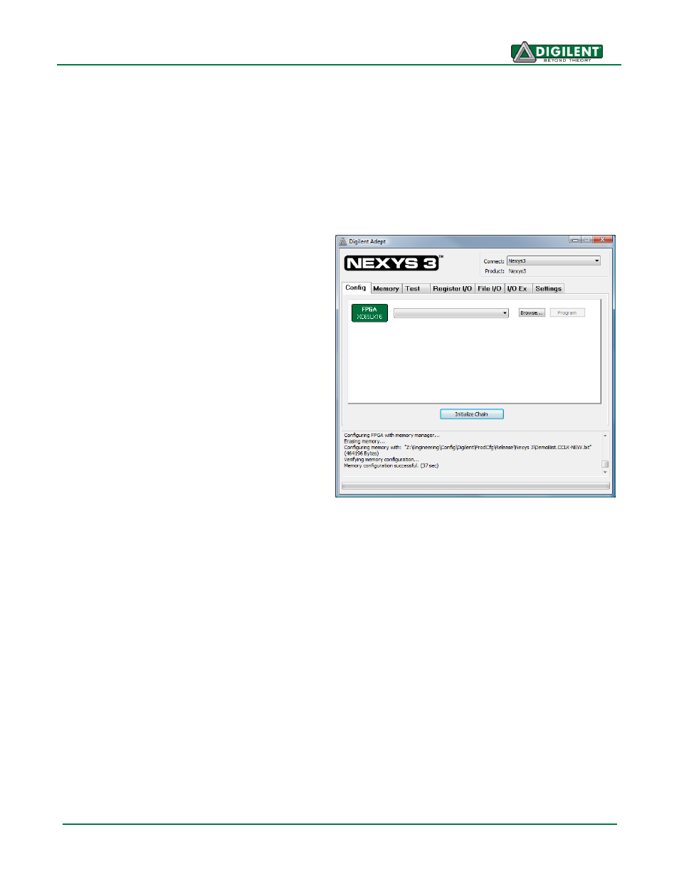
Programming Interface
To program the Nexys3 board using Adept, first
set up the board and initialize the software:
plug in and attach the power supply
plug in the USB cable to the PC and to
the USB port on the board
start the Adept software
turn ON Nexys3's power switch
wait for the FPGA to be recognized.
Use the browse function to associate the
desired .bit file with the FPGA, and click on the
Program button. The configuration file will be
sent to the FPGA, and a dialog box will indicate
whether programming was successful. The
configuration “done” LED will light after the
FPGA has been successfully configured.
Before starting the programming sequence, Adept ensures that any selected configuration file
contains the correct FPGA ID code
– this prevents incorrect .bit files from being sent to the FPGA.
In addition to the navigation bar and browse and program buttons, the Config interface provides an
Initialize Chain button, console window, and status bar. The Initialize Chain button is useful if USB
communications with the board have been interrupted. The console window displays current status,
and the status bar shows real-time progress when downloading a configuration file.
Memory Interface
The Memory tab allows .bin, .bit, and .mcs
configuration files to be transferred to the on-
board BPI (parallel) or SPI (serial) PCM devices
for subsequent FPGA programming, and allows
user data files to be transferred to/from the
PCM devices or RAM memories at user-
specified addresses. The target memory is
selected by clicking one of the three radio
buttons in the upper-right corner.