Expansion connectors – Digilent 410-182P-KIT User Manual
Page 20
Nexys3 Reference Manual
Doc: 502-182
page 20 of 22
asserted, then a “7” will be displayed in digit position 2. If AN0 and CB, CC are driven for 4ms, and
then A1 and CA, CB, CC are driven for 4ms in an endless succession, the display will show “17” in the
first two digits. An example timing diagram for a four-digit controller is provided.
Expansion Connectors
The Nexys3 board has a 68-pin VHDC connector for high-speed/parallel I/O, and an 8-pin Pmod
connector for lower speed and lower pin-count I/O.
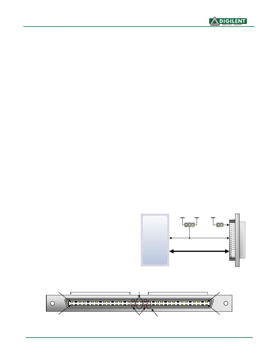
VHDC Connector
The VHDC connector includes 40 data signals (routed as 20 impedance-controlled matched pairs), 20
grounds (one per pair), and eight power signals. This connector, commonly used for SCSI-3
applications, can accommodate data rates of several hundred megahertz on every pin. Both board-to-
board and board-to-cable mating connectors are available. Data sheets for the VHDC connector and
for mating board and cable connectors can be found on the Digilent website, as well as on other
vendor and distributor websites. Mating connectors and cables of various lengths are also available
from Digilent and from distributors.
All FPGA pins routed to the VHDC connector are located in FPGA I/O bank0. The FPGA's bank0 I/O
power supply pins and the VHDC connector's four Vcc pins are connected together by a small,
segregated power supply plane in the PCB. This sub-plane can be connected to 2.5V or 3.3V,
depending on the position of jumper JP8. This arrangement allows peripheral boards and the FPGA to
share the same Vcc and signaling voltage across the connector, whether it be 3.3V or 2.5V.
The unregulated board voltage VU5V0 (nominally 5V) is also routed to four other VHDC pins,
supplying up to 1A of additional current to peripheral boards. A second jumper (JP4) allows the
unregulated board voltage to be disconnected
from the VHDC connector if desired.
A
ll I/O’s to the VHDC connector are routed as
matched pairs to support LVDS signaling,
commonly powered at 2.5V. The connector
uses a symmetrical pinout (as reflected around
the connector's vertical axis) so that peripheral
boards as well as other system boards can be
connected. Connector pins 15 and 49 are
routed to FPGA clock input pins.
VU
Pin 34
Pin 68
Pin 1:IO1-P
Pin 35:IO1-N
VCC
10 Matched Pairs
10 Matched Pairs
Clock Inputs
3.3V 2.5V
Spartan 6
VHDC
VCCO
20 Matched Pairs
JP8
VU5V0
Bank0
JP4