1 ddr2 – Digilent 410-292P-KIT User Manual
Page 7
Nexys4 DDR™ FPGA Board Reference Manual
Copyright Digilent, Inc. All rights reserved.
Other product and company names mentioned may be trademarks of their respective owners.
Page 7 of 29
In case of an error during configuration, the LED will blink rapidly.
When the FPGA has been successfully configured, the behavior of the LED is application-specific. For example, if a
USB keyboard is plugged in, a rapid blink will signal the receipt of an HID input report from the keyboard.
4
Memory
The Nexys4 DDR board contains two external memories: a 1Gib (128MiB) DDR2 SDRAM and a 128Mib (16MiB)
non-volatile serial Flash device. The DDR2 modules are integrated on-board and connect to the FPGA using the
industry standard interface. The serial Flash is on a dedicated quad-mode (x4) SPI bus. The connections and pin
assignments between the FPGA and external memories are shown below.
4.1 DDR2
The Nexys4 DDR includes one Micron MT47H64M16HR-25:H DDR2 memory component, creating a single rank, 16-
bit wide interface. It is routed to a 1.8V-powered HR (High Range) FPGA bank with 50 ohm controlled single-ended
trace impedance. 50 ohm internal terminations in the FPGA are used to match the trace characteristics. Similarly,
on the memory side, on-die terminations (ODT) are used for impedance matching.
For proper operation of the memory, a memory controller and physical layer (PHY) interface needs to be included
in the FPGA design. There are two recommended ways to do that, which are outlined below and differ in
complexity and design flexibility.
The straightforward way is to use the Digilent-provided DDR-to-SRAM adapter module which instantiates the
memory controller and uses an asynchronous SRAM bus for interfacing with user logic. This module provides
backward compatibility with projects written for older Nexys-line boards featuring a CellularRAM instead of DDR2.
It trades memory bandwidth for simplicity.
More advanced users or those who wish to learn more about DDR SDRAM technology may want to use the Xilinx
7-series memory interface solutions core generated by the MIG (Memory Interface Generator) Wizard. Depending
on the tool used (ISE, EDK or Vivado), the MIG Wizard can generate a native FIFO-style or an AXI4 interface to
connect to user logic. This workflow allows the customization of several DDR parameters optimized for the
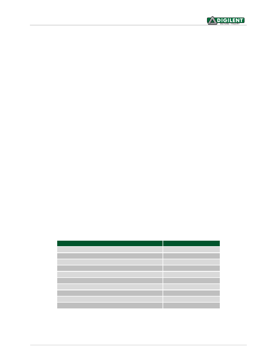
particular application. Table 2 below lists the MIG Wizard settings optimized for the Nexys4 DDR.
Setting
Value
Memory type
DDR2 SDRAM
Max. clock period
3000ps (667Mbps data rate)
Recommended clock period (for easy clock generation) 3077ps (650Mbps data rate)
Memory part
MT47H64M16HR-25E
Data width
16
Data mask
Enabled
Chip Select pin
Enabled
Rtt (nominal) – On-die termination
50ohms
Internal Vref
Enabled
Internal termination impedance
50ohms
Table 2. DDR2 settings for the Nexys4 DDR.
Although the FPGA, memory IC, and the board itself are capable of the maximum data rate of 667Mbps, the
limitations in the clock generation primitives restrict the clock frequencies that can be generated from the 100
MHz system clock. Thus, for simplicity, the next highest data rate of 650Mbps is recommended.