Digilent 410-292P-KIT User Manual
Page 2
Nexys4 DDR™ FPGA Board Reference Manual
Copyright Digilent, Inc. All rights reserved.
Other product and company names mentioned may be trademarks of their respective owners.
Page 2 of 29
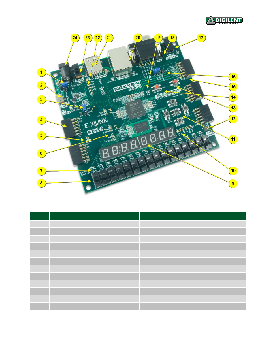
Callout
Component Description
Callout
Component Description
1
Power select jumper and battery header
13
FPGA configuration reset button
2
Shared UART/ JTAG USB port
14
CPU reset button (for soft cores)
3
External configuration jumper (SD / USB)
15
Analog signal Pmod connector (XADC)
4
Pmod connector(s)
16
Programming mode jumper
5
Microphone
17
Audio connector
6
Power supply test point(s)
18
VGA connector
7
LEDs (16)
19
FPGA programming done LED
8
Slide switches
20
Ethernet connector
9
Eight digit 7-seg display
21
USB host connector
10
JTAG port for (optional) external cable
22
PIC24 programming port (factory use)
11
Five pushbuttons
23
Power switch
12
Temperature sensor
24
Power jack
A growing collection of board support IP, reference designs, and add-on boards are available on the Digilent
website. See the Nexys4 DDR page a
for more information.
Figure 1. Nexys4 DDR board features.