1 jtag configuration – Digilent 410-292P-KIT User Manual
Page 5
Nexys4 DDR™ FPGA Board Reference Manual
Copyright Digilent, Inc. All rights reserved.
Other product and company names mentioned may be trademarks of their respective owners.
Page 5 of 29
M0
M1
JTAG
Port
USB
Controller
SPI Quad mode
Flash
1x6 JTAG
Header
SPI
Port
Micro-AB USB
Connector (J6)
USB-JTAG/UART Port
Artix-7
Done
PIC24
Type A USB Host
Connector (J5)
Serial
Prog. Port
2
6-pin JTAG
Header (J10)
Prog
Micro SD
Connector (J1)
Media Select
(JP2)
User I/O
M2
Mode (JP1)
Programming Mode
JP2
JP1
NA
SPI Flash
NA
JTAG
USB
MicroSD
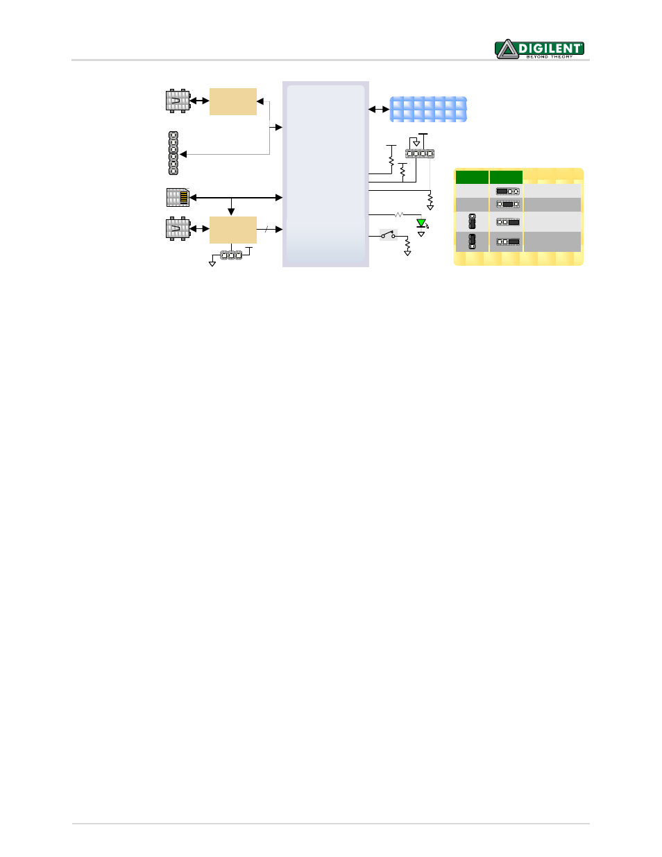
Figure 3. Nexys4 DDR configuration options.
Figure 3 shows the different options available for configuring the FPGA. An on-board “mode” jumper (JP1) and a
media selection jumper (JP2) select between the programming modes.
The FPGA configuration data is stored in files called bitstreams that have the .bit file extension. The ISE or Vivado
software from Xilinx can create bitstreams from VHDL, Verilog®, or schematic-based source files (in the ISE toolset,
EDK is used for MicroBlaze™ embedded processor-based designs).
Bitstreams are stored in SRAM-based memory cells within the FPGA. This data defines the FPGA’s logic functions
and circuit connections, and it remains valid until it is erased by removing board power, by pressing the reset
button attached to the PROG input, or by writing a new configuration file using the JTAG port.
An Artix-7 100T bitstream is typically 30,606,304 bits and can take a long time to transfer. The time it takes to
program the Nexys4 can be decreased by compressing the bitstream before programming, and then allowing the
FPGA to decompress the bitstream itself during configuration. Depending on design complexity, compression
ratios of 10x can be achieved. Bitstream compression can be enabled within the Xilinx tools (ISE or Vivado) to occur
during generation. For instructions on how to do this, consult the Xilinx documentation for the toolset being used.
After being successfully programmed, the FPGA will cause the "DONE" LED to illuminate. Pressing the “PROG”
button at any time will reset the configuration memory in the FPGA. After being reset, the FPGA will immediately
attempt to reprogram itself from whatever method has been selected by the programming mode jumpers.
The following sections provide greater detail about programming the Nexys4 DDR using the different methods
available.
3.1 JTAG Configuration
The Xilinx tools typically communicate with FPGAs using the Test Access Port and Boundary-Scan Architecture,
commonly referred to as JTAG. During JTAG programming, a .bit file is transferred from the PC to the FPGA using
the onboard Digilent USB-JTAG circuitry (port J6) or an external JTAG programmer, such as the Digilent JTAG-HS2,
attached to port J10. You can perform JTAG programming any time after the Nexys4 DDR has been powered on,
regardless of what the mode jumper (JP1) is set to. If the FPGA is already configured, then the existing
configuration is overwritten with the bitstream being transmitted over JTAG. Setting the mode jumper to the JTAG