12 microsd slot, 13 temperature sensor, 1 i2c interface – Digilent 410-292P-KIT User Manual
Page 22: Artix-7
Nexys4 DDR™ FPGA Board Reference Manual
Copyright Digilent, Inc. All rights reserved.
Other product and company names mentioned may be trademarks of their respective owners.
Page 22 of 29
XADC core is controlled and accessed from a user design via the Dynamic Reconfiguration Port (DRP). The DRP also
provides access to voltage monitors that are present on each of the FPGA’s power rails, and a temperature sensor
that is internal to the FPGA. For more information on using the XADC core, refer to the Xilinx document titled “7
Series FPGAs and Zynq-7000 All Programmable SoC XADC Dual 12-Bit 1 MSPS Analog-to-Digital Converter.”
12 MicroSD Slot
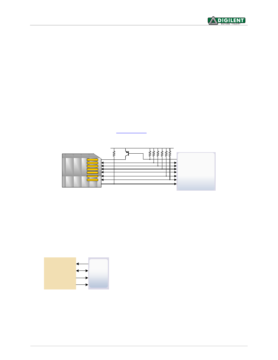
The Nexys4 DDR provides a microSD slot for both FPGA configuration and user access. The on-board Auxiliary
Function microcontroller shares the SD card bus with the FPGA. Before the FPGA is configured the microcontroller
must have access to the SD card via SPI. Once a bit file is downloaded to the FPGA (from any source), the
microcontroller power cycles the SD slot and relinquishes control of the bus. This enables any SD card in the slot to
reset its internal state machines and boot up in SD native bus mode. All of the SD pins on the FPGA are wired to
support full SD speeds in native interface mode, as shown in Figure 21. The SPI is also available, if needed. Once
control over the SD bus is passed from the microcontroller to the FPGA, the SD_RESET signal needs to be actively
driven low by the FPGA to power the microSD card slot. For information on implementing an SD card controller,
refer to the SD card specification available a
Artix-7
A1
SD MICRO (J1)
VDD
DAT2
DAT1
CMD
CLK
DAT3
DAT0
CARD_DETECT
3.3V
SD_RESET
C2
D2
B1
C1
E1
F1
E2
Figure 21. Artix-7 microSD card connector interface (PIC24 connections not shown).
13 Temperature Sensor
The Nexys4 DDR includes an Analog Device ADT7420 temperature sensor. The sensor provides up to 16-bit
resolution with a typical accuracy better than 0.25 degrees Celsius. The interface between the temperature sensor
and FPGA is shown in Figure 22.
Artix 7
ADT7420
SDA
TMP_INT
TMP_CT
C15
D13
B14
SCL: I2C Serial Clock
SDA: I2C Serial Data
TMP_INT: Over-temperature and Under-temperature Indicator
C14
SCL
TMP_CT: Critical Over-temperature Indicator
Figure 22. Temperature sensor interface.
13.1 I2C Interface
The ADT7420 chip acts as a slave device using the industry standard I2C communication scheme. To communicate
with ADT7420 chip, the I2C master must specify a slave address (0x4B) and a flag indicating whether the