9vga port, 1 vga system timing, Artix-7 – Digilent 410-292P-KIT User Manual
Page 14
Nexys4 DDR™ FPGA Board Reference Manual
Copyright Digilent, Inc. All rights reserved.
Other product and company names mentioned may be trademarks of their respective owners.
Page 14 of 29
9
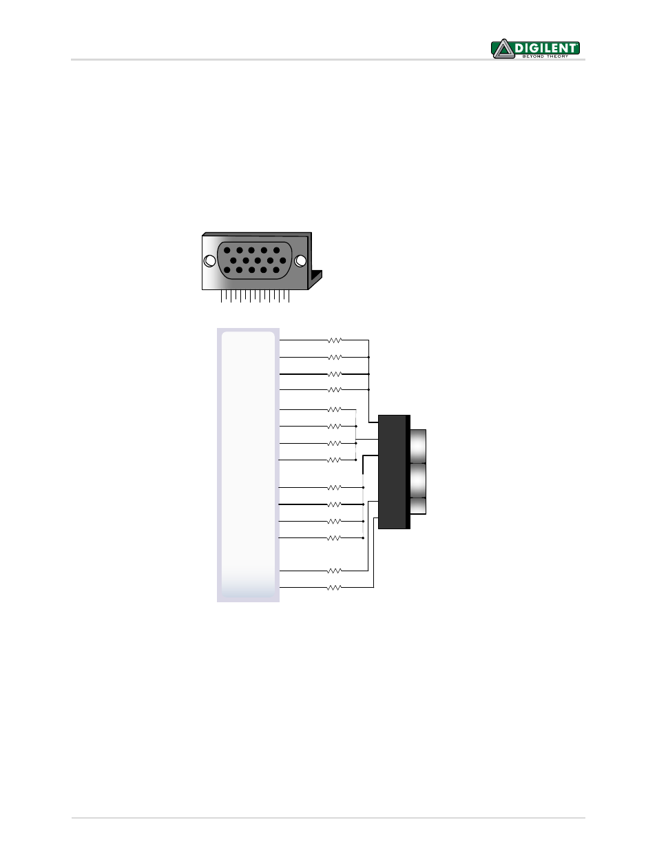
VGA Port
The Nexys4 DDR board uses 14 FPGA signals to create a VGA port with 4 bits-per-color and the two standard sync
signals (HS – Horizontal Sync, and VS – Vertical Sync). The color signals use resistor-divider circuits that work in
conjunction with the 75-ohm termination resistance of the VGA display to create 16 signal levels each on the red,
green, and blue VGA signals. This circuit, shown in Figure 11, produces video color signals that proceed in equal
increments between 0V (fully off) and 0.7V (fully on). Using this circuit, 4096 different colors can be displayed, one
for each unique 12-bit pattern. A video controller circuit must be created in the FPGA to drive the sync and color
signals with the correct timing in order to produce a working display system.
9.1 VGA System Timing
VGA signal timings are specified, published, copyrighted, and sold by the VESA® organization (www.vesa.org). The
following VGA system timing information is provided as an example of how a VGA monitor might be driven in 640
by 480 mode.
NOTE: For more precise information, or for information on other VGA frequencies, refer to documentation
available at the VESA website.
Figure 11. Nexys4 DDR VGA interface.
HD-DB15
4K
W
2K
W
1K
W
100
W
100
W
15
10
5
11
6
1
Pin 1: Red
Pin 2: Grn
Pin 3: Blue
Pin 13: HS
Pin 14: VS
Pin 5: GND
Pin 6: Red GND
Pin 7: Grn GND
Pin 8: Blu GND
Pin 10: Sync GND
RED0
RED1
RED2
4K
W
2K
W
1K
W
GRN0
GRN1
GRN2
RED
GRN
BLU
HS
VS
Artix-7
A3
B4
C5
B11
C6
A5
B6
B12
HSYNC
VSYNC
510
W
RED3
A4
510
W
GRN3
A6
4K
W
2K
W
1K
W
BLU0
BLU1
BLU2
510
W
BLU3
B7
C7
D7
D8