10 basic i/o – Digilent 410-292P-KIT User Manual
Page 17

Nexys4 DDR™ FPGA Board Reference Manual
Copyright Digilent, Inc. All rights reserved.
Other product and company names mentioned may be trademarks of their respective owners.
Page 17 of 29
T
S
T
disp
T
pw
T
fp
T
bp
T
S
T
disp
T
pw
T
fp
T
bp
Sync pulse
Display time
Pulse width
Front porch
Back porch
16.7ms
15.36ms
64 us
320 us
928 us
416,800
384,000
1,600
8,000
23,200
521
480
2
10
29
Symbol
Parameter
Time
Clocks Lines
Vertical Sync
32 us
25.6 us
3.84 us
640 ns
1.92 us
800
640
96
16
48
Clks
Horiz. Sync
Time
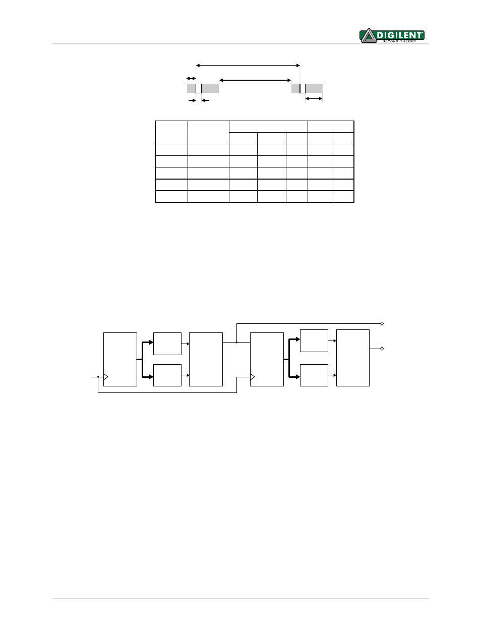
Figure 14. Signal timings for a 640-pixel by 480 row display using a 25 MHz pixel clock and 60 Hz vertical refresh.
A VGA controller circuit, such as the one diagramed in Figure 15, decodes the output of a horizontal-sync counter
driven by the pixel clock to generate HS signal timings. You can use this counter to locate any pixel location on a
given row. Likewise, the output of a vertical-sync counter that increments with each HS pulse can be used to
generate VS signal timings, and you can use this counter to locate any given row. These two continually running
counters can be used to form an address into video RAM. No time relationship between the onset of the HS pulse
and the onset of the VS pulse is specified, so you can arrange the counters to easily form video RAM addresses, or
to minimize decoding logic for sync pulse generation.
Horizontal
Counter
Zero
Detect
3.84us
Detect
Horizontal
Synch
Set
Reset
Vertical
Counter
Zero
Detect
64us
Detect
Vertical
Synch
Set
Reset
CE
VS
HS
Pixel
CLK
Figure 15. VGA display controller block diagram.
10 Basic I/O
The Nexys4 DDR board includes two tri-color LEDs, sixteen slide switches, six push buttons, sixteen individual LEDs,
and an eight-digit seven-segment display, as shown in Figure 16. The pushbuttons and slide switches are
connected to the FPGA via series resistors to prevent damage from inadvertent short circuits (a short circuit could
occur if an FPGA pin assigned to a pushbutton or slide switch was inadvertently defined as an output). The five
pushbuttons arranged in a plus-sign configuration are "momentary" switches that normally generate a low output
when they are at rest, and a high output only when they are pressed. The red pushbutton labeled “CPU RESET,” on
the other hand, generates a high output when at rest and a low output when pressed. The CPU RESET button is
intended to be used in EDK designs to reset the processor, but you can also use it as a general purpose
pushbutton. Slide switches generate constant high or low inputs depending on their position.
