Vmp1 configuration – Kontron VMP1 User Manual
Page 57
VMP1
Configuration
ID 19972, Rev. 0101
Page 4 - 11
® PEP Modular Computers GmbH
4.3.4.4 Memory Configuration Register
•
Bits SZ0 and SZ1 are used to identify the soldered SDRAM size.
•
Bit 2 and Bit 3 are reserved
•
Bit 4 (ECC) is used to indicate that ECC is supported (1 = ECC enabled)
•
Bit MSB (BJ) indicates the status of the BOOT JUMPER (jumper J1 for exchang-
ing Socket and Flash Chip Select). 0 = boot jumper set, 1 = boot jumper removed
4.3.4.5 SDRAM Size
4.3.4.6 Flash Bank Select Register
The Flash bank select register is used to select the appropriate Flash bank. As 8-bit
wide Flash memory may only be accessed through a 512 kB window; this is the only
way to address a larger size Flash memory. Using bits FB0..FB3, 16 Flash banks can be
selected (16x512 kB = 8 MB). The default value on startup of the VMP1 is 0x00.
Table 4-9: Memory Configuration Register
Register
Address
MSB
6
5
4
3
2
1
LSB
Memory Configuration
FFe0 0014
BJ
Res.
Res.
ECC
Res.
Res.
SZ1
SZ0
Table 4-10: SDRAM Size
SZ1
SZ0
Meaning
0
0
32 MB/1 Bank
0
1
64 MB/2 Banks
1
0
Reserved
1
1
Reserved
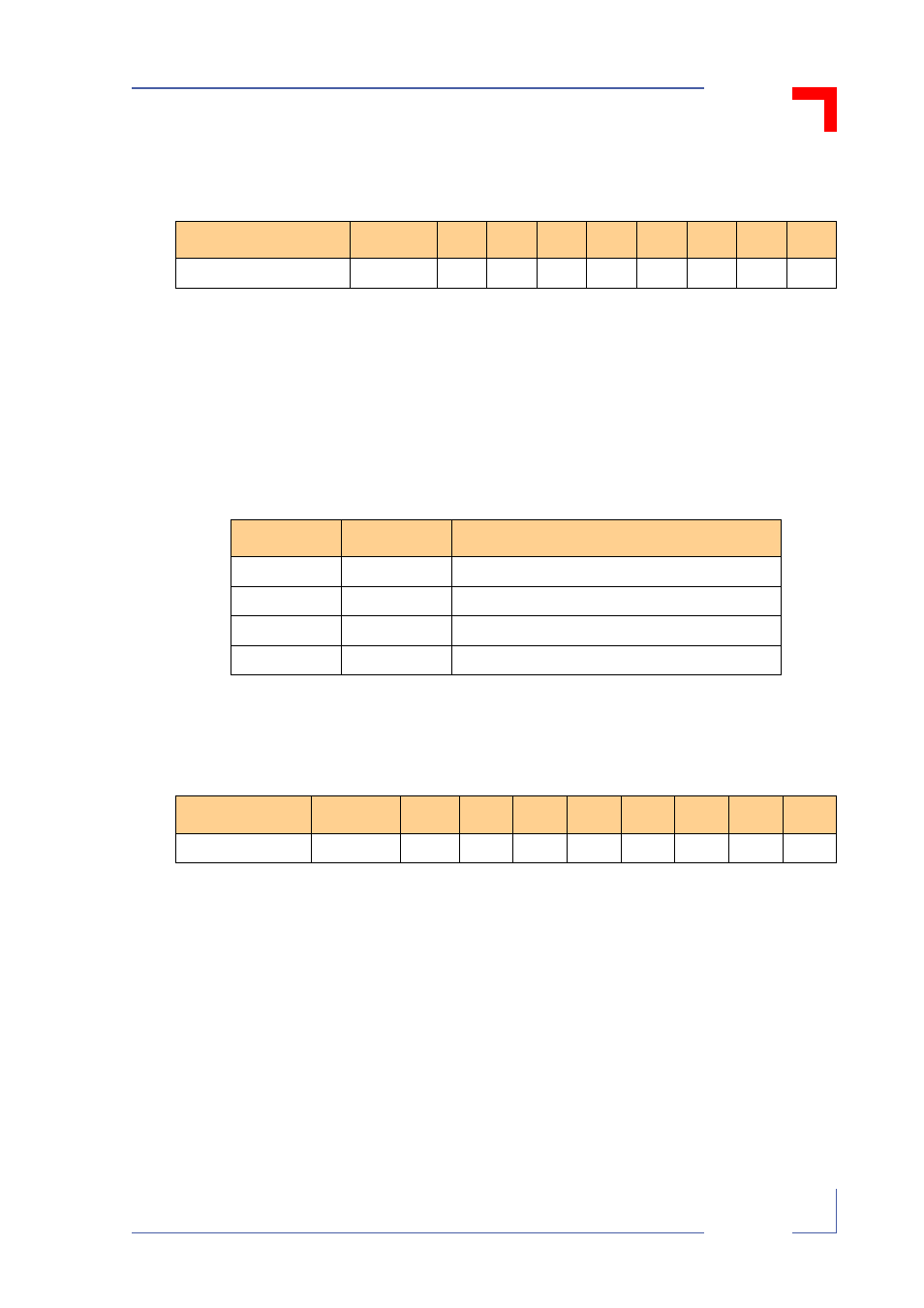
Table 4-11: Flash Bank Select Register
Register
Address
MSB
6
5
4
3
2
1
LSB
Flash bank select
FFe0 0016
Res.
Res.
Res.
Res.
FB3
FB2
FB1
FB0