Byte-lane clocks, Io ring – Achronix Speedster22i Clock and Reset Networks User Manual
Page 20
20
UG027, May 21, 2014
Byte-Lane Clocks
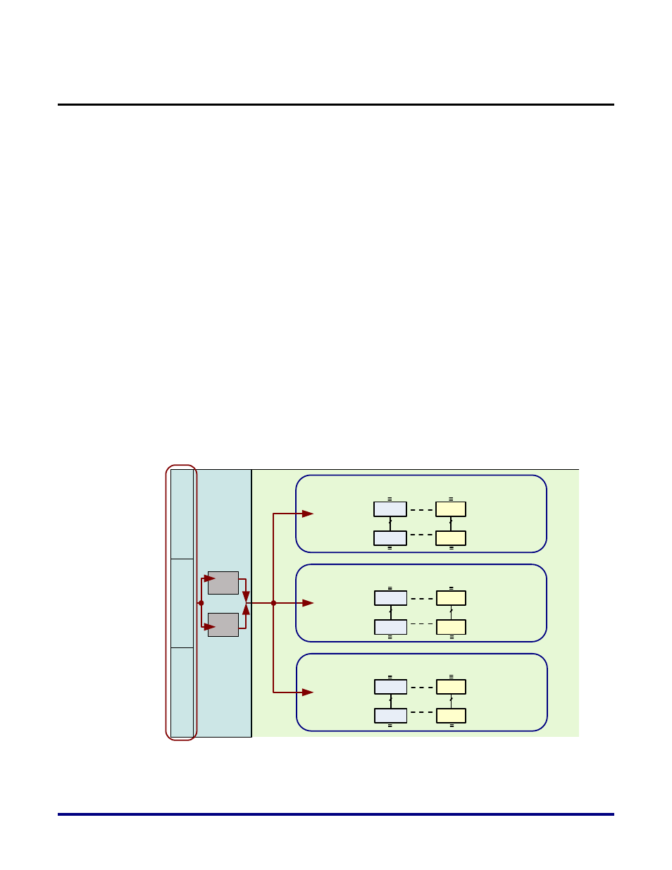
For source synchronous transfers, where data and clock are both sent from the IO ring to the
core, using one of the clock networks as described above would result in a large skew
between the data and the clock.
For this reason, there is a dedicated entry point from the byte lanes into the clock inputs of
the clock regions, via the data interconnect route in the fabric into the CRMU. These are
known as byte-lane clocks and are predominantly used to forward data strobe (dqs) clock
signals from the PHY into the FPGA fabric. A byte lane in a Speedster22i FPGA consists of 12
I/O buffers. For every set of 13 byte-lanes making up an IO cluster, (which corresponds to the
IOs used in the hard DDR3 controllers), there is a clock signal that is used for sampling the
data at the IO PHY. This clock signal can go through 2 clock dividers, a divide-by-2 clock
module and a divide-by-4 clock module. The outputs of these modules, which correspond to
the half-rate or quarter-rate clocks in a memory interface application can be forwarded to the
3 clock regions corresponding to that IO site. Note that for memory interface applications,
usage of mesochronous synchronizers in the Rx datapath will allow for clock domain
crossing between the dqs clock domain and a core clock network, eliminating the need for
clock forwarding into the fabric. For more details, please refer to the Memory PHY User
Guide.
Figure 11 below illustrates the the entry point of these byte-lane clocks into a clock region in
the WN site of the device. These clocks are muxed with the clocks coming from the CRMU
and are then fed to all of the blocks in the fabric IP column.
B
y
te
-L
a
n
e
s
0
-3
B
y
te
L
a
n
e
s
4
-7
B
y
te
L
a
n
e
s
8
-1
2
Core Fabric
W
e
s
t-
N
o
rt
h
(
W
N
)
IO
C
lu
s
te
r
Clock Region West 1
Clock Region West 2
Clock Region West 3
RLBs
RLBs
MULTs
MULTs
16
16
RLBs
RLBs
MULTs
MULTs
16
16
RLBs
RLBs
MULTs
MULTs
16
16
Clk
div4
Clk
div2
IO Ring
Figure 11: Byte-Lane Clocks in a Clock Region