Core clock network components, Clock generator (cg), Serdes – Achronix Speedster22i Clock and Reset Networks User Manual
Page 10
10
UG027, May 21, 2014
Core Clock Network Components
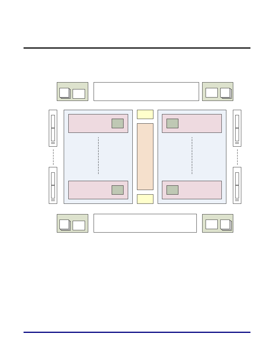
Figure 3 provides block level highlights of the different core clock network components on
the Speedster 22iHD FPGA. These are color coded to better distinguish between them. The
sections below provide more in depth explanations of these different components.
SerDes
PLL
GCGs
PLL
PLLs
Clock
Buffers
PLL
GCGs
PLL
PLLs
Clock
Buffers
PLL
GCGs
PLL
PLLs
SerDes
Clock
Buffers
PLL
GCGs
PLL
PLLs
Clock
Buffers
I/O
Bank
B
y
te
L
a
n
e
s
B
y
te
L
a
n
e
s
I/O
Bank
B
y
te
L
a
n
e
s
B
y
te
L
a
n
e
s
I/O
Bank
B
y
te
L
a
n
e
s
B
y
te
L
a
n
e
s
I/O
Bank
B
y
te
L
a
n
e
s
B
y
te
L
a
n
e
s
Clock Region W1
Clock Region Wn
Clock Region E1
Clock Region En
Clock
Hub
Clock Mux
Top
Clock Mux
Bottom
CRMU
Wn
CRMU
E1
CRMU
En
CRMU
W1
Figure 3: Core Clock Network Components on the FPGA
Clock Generator (CG)
There are four Clock Generators (CGs) on a Speedster 22iHD FPGA, one in each corner of the
device. Each CG contains six clock I/O buffers (CBs) and four Phase Locked Loops (PLLs) and
each PLL has four output counters.
The six clock buffers can be used either as three differential I/Os or six single‐ended I/Os. If
these I/Os are not used as clock buffers, they can be used as generic inputs or outputs. These
buffers can be easily identified in the pin table or the package spreadsheet provided by ACE,
by filtering the USE column to show the clock pins. Each of these clock pins can be uniquely
identified by referencing one of the four bank locations (CB0, CB1, CB2 and CB3
corresponding to NW, SW, SE and NE respectively) as well as the pad number (0-6). The
table snapshot from the package spreadsheet below illustrates these concepts.