Clock hub – Achronix Speedster22i Clock and Reset Networks User Manual
Page 15
UG027, May 21, 2014
15
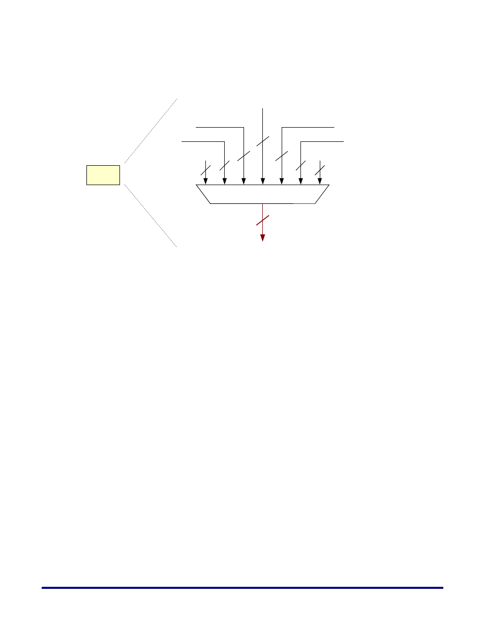
into the clock hub. Figure 6 below provides a detailed view of the internals of the clock mux
located at the top center of the device.
Clock Mux
Top
6
16
16
6
16
16
52
128 to 32 Fully
General Crossbar
From Top SerDes Lanes
32
From NW Clock Generator through
Global Boundary Clock
From NW Clock Generator through
Local Boundary Clock
To Clock Hub
No Connect
No Connect
From NE Clock Generator through
Global Boundary Clock
From NE Clock Generator through
Local Boundary Clock
Figure 6: Detailed View of the Top Clock Mux
Clock Hub
The clock hub in the center of the device collects the two 32-bit buses coming in from the top
and bottom clock muxes, as well as a 16-bit bus from the data interconnect to generate the 48-
bit global clock bus.
The 48-bit global clock bus (shown in green) travels back up and down the length of the clock
hub to feed each of the clock regions.
The 32-bit buses coming in from the top and bottom (shown in red) are actually also the
direct core clocks which are tapped off at each of the clock regions. A 12-bit subset of this 32-
bit bus is selected as shown in Figure 7 below.
The 16-bit bus coming in from the data interconnect (shown in blue), is one of the ways of
getting a signal from data generated in the FPGA fabric into a clock network, and this path is
the only way of generating a global core clock signal from the interconnect data.
Figure 7 below provides a detailed view of the clock hub.