Rockwell Automation System Design for the Control of Electrical Noise User Manual
Page 22

Publication GMC-RM001A-EN-P — July 2001
2-4
High Frequency (HF) Bonding
The ground plane principle was originally developed by printed
circuit board (PCB) designers for high frequency circuits. In
multi-layer PCBs a minimum of two copper layers are used with one
being designated the ground or common. This layer covers as large an
area as possible and each IC common is tied directly to it. In addition,
each IC Vss (+5V) pin is decoupled by a 0.1
µ
F capacitor to the
ground plane as close as possible to the pin. The capacitor presents a
very low impedance at RF hence any induced noise current generates
minimal voltage.
The fundamental property of a ground plane is that every point on its
surface is at the same potential (and zero impedance) at all
frequencies. At high frequencies this is more effective than the use of
single point grounding schemes. This is because wire has significant
inductance at RF and just a few inches can create an unacceptable
voltage drop. Refer to the section Bonding Surfaces in Appendix A for
more information.
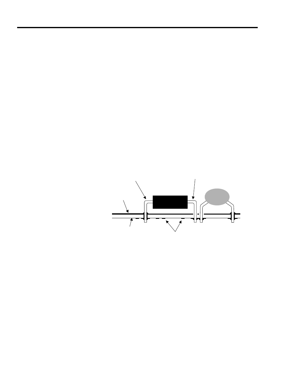
Figure 2.3
Ground plane layer in a double-sided printed circuit board
Ground plane construction has proved so successful that it is now
universal in PCB design for all but the most price-sensitive and low
frequency circuits. Single-sided PCBs are not generally used for RF or
TTL circuits.
Integrated Circuit
Decoupling Capacitor
(Vss to ground)
Ground plane
layer
Interconnect
layer
Vdd pin
(common)
Vss pin
(+5V)
Insulation
layer
