Rockwell Automation 1794-IF4I, -OF4I, IF2XOF2I, -IF4IXT, -IF4ICFXT, -OF4IXT, IF2XOF2IXT FLEX I/O Isolated Analog Modules User Manual
Page 74
Publication 1794-6.5.8 - January 2010
74 Writing Configuration to and Reading Status from Your Module with a Remote I/O Adapter
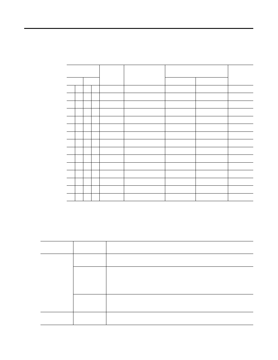
Table 4.19
Configuring Your Outputs for the 1794-IF2XOF2I Analog Combo Module
Configuration
Bits
Nominal
Range
Data Type
Output Values
(1)
Update
Rate
MSD
LSD
Hexadecimal
Decimal
0
0
0
1
4-20mA
2’s complement
<0000–7878>
<0000–30840>
5.0ms
0
0
1
0
±10V
2’s complement
<8618–79E8>
<–31208–31208> 2.5ms
0
0
1
1
±5V
2’s complement
<8618–79E8>
<–31208–31208> 2.5ms
0
1
0
0
0-20mA
2’s complement %
0–2710>
0–10000>
5.0ms
0
1
0
1
4-20mA
2’s complement %
<0–2710>
<0–10000>
5.0ms
0
1
1
0
0-10V
2’s complement %
0–2710>
0–10000>
5.0ms
0
1
1
1
±10V
2’s complement %
<–D8F0–2710>
<–10000–10000> 5.0ms
1
0
0
0
0-20mA
binary
0000–F3CF>
0000–62415>
2.5ms
1
0
0
1
4-20mA
binary
0000–F0F1>
0000–61681>
5.0ms
1
0
1
0
0–10V
binary
0000–F3CF>
0000–62415>
2.5ms
1
0
1
1
0-5V
binary
0000–F3CF>
0000–62415>
2.5ms
1
1
0
0
±20mA
offset binary
8000–F9E8>
32768–63976>
2.5ms
1
1
0
1
4-20mA
offset binary
<8000–F878>
<32768–63608>
5.0ms
1
1
1
0
±10V
offset binary
<0618–F9E8>
<1560–63976>
2.5ms
1
1
1
1
±5V
offset binary
<0618–F9E8>
<1560–63976>
2.5ms
(1)
< and > indicate the overrun beyond actual range (about 5%).
Table 4.20
Word/Bit Descriptions for the 1794-IF2XOF2I Analog Combo
Module Write
Write Word
Decimal Bit
(Octal Bit)
Definition
Word 0
Bits 00–14
(00–16)
Not used
Bit 13–14 (15–16) Safe State Source bits (S1/S0). – When EN is 0, these bits designate the source of
the safe state data.
Bit 13 = 0, bit 14 = 1 – reset outputs to 0V/0mA (used with 1794-ASB/C)
Bit 13 = 1, bit 14 = 1 – hold output at its current level (used with 1794-ASB/C)
Bit 13 = 0; bit 14 = 0 – Safe state data is in output data words
Bit 15 (17)
Output enable bit (EN). – When set (1), the outputs are enabled. This bit must be set
in order for the real time data to appear at the outputs. If this bit is not set (0), the
outputs will be determined by S1/S0.
Word 1
Bits 00–15
(00–17)
Output Channel 0 data. Refer to Table 4.19.