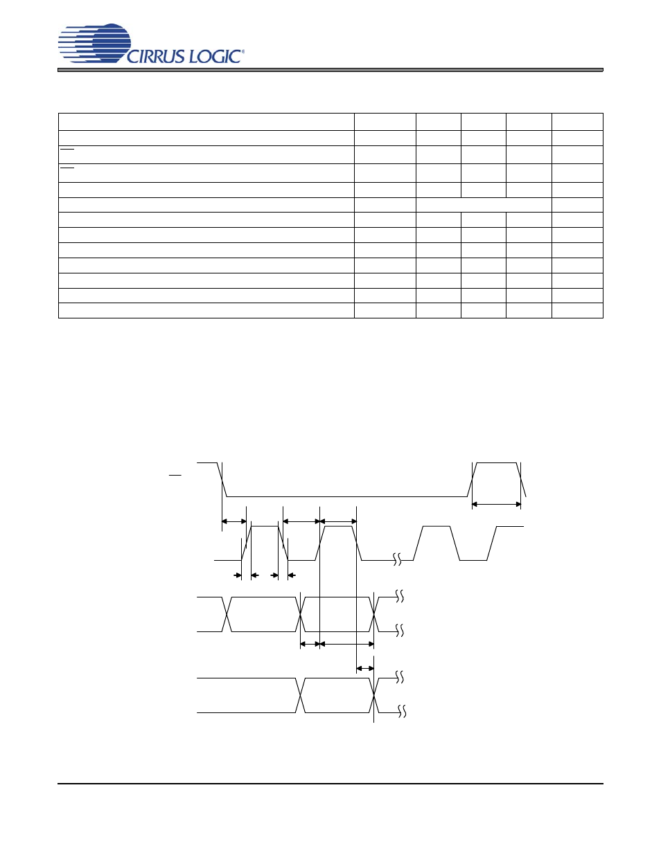
Figure 3. spi mode timing – Cirrus Logic CS8406 User Manual
Page 7
DS580F6
7
CS8406
SWITCHING CHARACTERISTICS - CONTROL PORT - SPI MODE
(Inputs: Logic 0 = 0 V, Logic 1 = VL; C
L
= 20 pF)
Notes:
9. If Fs is lower than 51.850 kHz, the maximum CCLK frequency should be less than 115 Fs. This is dic-
tated by the timing requirements necessary to access the Channel Status and User Bit buffer memory.
Access to the control register file can be carried out at the full 6 MHz rate.
10. T
sch
must be greater than the larger of the two values, either 1/256FS + 8 ns, or 66 ns.
11. Data must be held for sufficient time to bridge the transition time of CCLK.
12. For f
sck
< 1 MHz.
Parameter
Symbol
Min
Typ
Max
Units
CCLK Clock Frequency
f
sck
0
-
6.0
MHz
CS High Time Between Transmissions
t
csh
1.0
-
-
s
CS Falling to CCLK Edge
t
css
20
-
-
ns
CCLK Low Time
t
scl
66
-
-
ns
CCLK High Time
t
sch
MAX ((1/256 F
S
+ 8), 66)
ns
CDIN to CCLK Rising Setup Time
t
dsu
40
-
-
ns
CCLK Rising to DATA Hold Time
t
dh
15
-
-
ns
CCLK Falling to CDOUT Stable
t
pd
-
-
50
ns
Rise Time of CDOUT
t
r1
-
-
25
ns
Fall Time of CDOUT
t
f1
-
-
25
ns
Rise Time of CCLK and CDIN
t
r2
-
-
100
ns
Fall Time of CCLK and CDIN
t
f2
-
-
100
ns
t r2
t f2
t dsu
t dh
t sch
t scl
CS
CCLK
CDIN
t css
t pd
CDOUT
tcsh
Figure 3. SPI Mode Timing