2 i·c mode, 2 i²c mode, Cs8406 – Cirrus Logic CS8406 User Manual
Page 17
DS580F6
17
CS8406
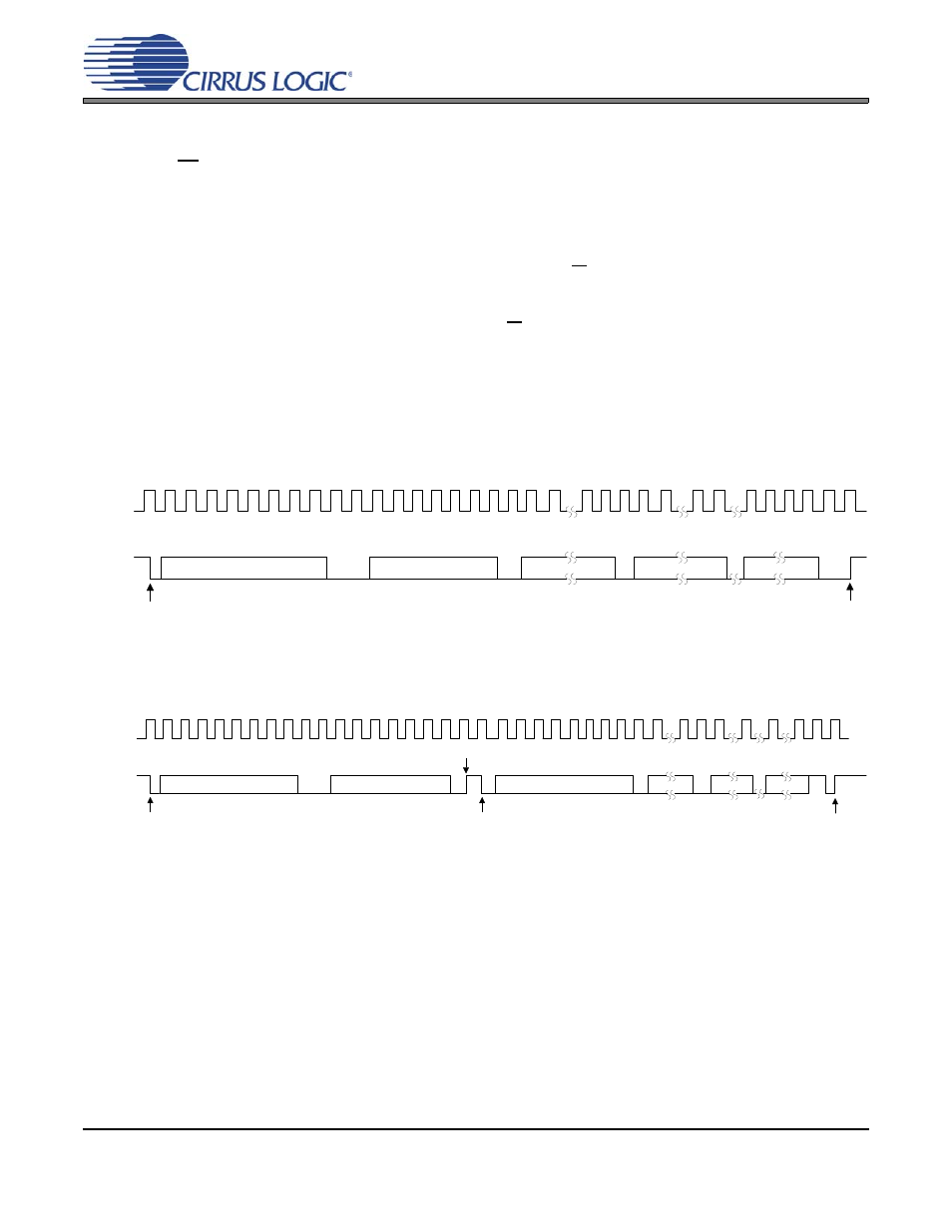
6.2
I²C Mode
In I²C Mode, SDA is a bidirectional data line. Data is clocked into and out of the part by the clock, SCL. There
is no CS pin. Pins AD0, AD1, and AD2 form the three least significant bits of the chip address and should
be connected to VL or GND as desired.
The signal timing for both a read and write cycle are shown in
and
. A Start condition is
defined as a falling transition of SDA while the clock is high. A Stop condition is a rising transition while the
clock is high. All other transitions of SDA occur while the clock is low. The first byte sent to the CS8406 after
a Start condition consists of a 7 bit chip address field and a R/W bit (high for a read, low for a write). The
upper 4 bits of the 7-bit address field are fixed at 0010. To communicate with a CS8406, the chip address
field, which is the first byte sent to the CS8406, should match 0010 followed by the settings of the AD2, AD1,
and AD0 pins. The eighth bit of the address is the R/W bit. If the operation is a write, the next byte is the
Memory Address Pointer (MAP) which selects the register to be read or written. If the operation is a read,
the contents of the register pointed to by the MAP will be output. Th e MAP automatically increments, so
consecutive registers can read from or written to easily. Each byte is separated by an acknowledge bit
(ACK). The ACK bit is output from the CS8406 after each input byte is read, and is input to the CS8406 from
the microcontroller after each transmitted byte.
Since the read operation cannot set the MAP, an aborted write operation is used as a preamble. As shown
, the write operation is aborted after the acknowledge for the MAP by sending a stop condition.
4 5 6 7
24 25
SCL
0 0 1 0 AD2 AD1 AD0 0
CHIP ADDRESS (WRITE)
MAP
DATA
DATA +1
START
ACK
STOP
ACK
ACK
ACK
SDA
6 5 4 3 2 1
7 6 1 0
7 6 1 0
7 6 1 0
0 1 2 3
8 9
12
16 17 18 19
10 11
13 14 15
27 28
26
DATA +n
Figure 11. Control Port Timing, I²C Slave Mode Write
SCL
CHIP ADDRESS (WRITE)
MAP
DATA
DATA +1
START
ACK
STOP
ACK
ACK
ACK
SDA
6 5 4 3 2 1 0
CHIP ADDRESS (READ)
START
7 0
7 0
7 0
NO
16
8 9
12 13 14 15
4 5 6 7
0 1
20 21 22 23 24
26 27 28
2 3
10 11
17 18 19
25
ACK
DATA + n
STOP
0 0 1 0 AD2 AD1 AD0 0
0 0 1 0 AD2 AD1 AD0 1
Figure 12. Control Port Timing, I²C Slave Mode Read