Cirrus Logic CS61583 User Manual
Page 16
The first bit (shifted in first) selects between an
output-enabled state (bit set to 1) or high-imped-
ance state (bit set to 0). The second bit shifted in
contains the test data that may be output on the
pin. Therefore, two J-TCK cycles are required to
load test data for each output pin.
The bi-directional pins have three bits in the
BSR to define input, output high, output low, or
high impedance. The first bit shifted into the
BSR configures the output driver as high-imped-
ance (bit set to 0) or active (bit set to 1). The
second bit shifted into the BSR sets the output
value when the first bit is 1. The third bit cap-
tures the value of the pin. This pin may have its
value set externally as an input (if the first bit is
0) or set internally as an output (if the first bit is
1). To configure a pad as an input, the J-TDI
pattern is 0X0. To configure a pad as an output,
the J-TDI pattern is 1X1. Therefore, three J-TCK
cycles are required to load test data for each bi-
directional pin.
Device Identification Register: The DIR provides
the manufacturer, part number, and version of the
CS61583. This information can be used to verify
that the proper version or revision number has
been used in the system under test. The DIR is 32
bits long and is partitioned as shown in figure 11.
Data from the DIR is shifted out to J-TDO LSB
first.
Bypass Register: The Bypass register consists of
a single bit, and provides a serial path between
J-TDI and J-TDO, bypassing the BSR. This al-
lows bypassing specific devices during certain
board-level tests. This also reduces test access
times by reducing the total number of shifts re-
quired from J-TDI to J-TDO.
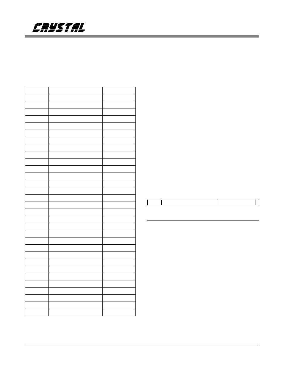
BIT #(s)
FUNCTION
Total Bits
31-28
Version number
4
27-12
Part Number
16
11-1
Manufacturer Number
11
0
Constant Logic ’1’
1
Figure 11. Device Identification Register
MSB
LSB
31
28 27
12 11
1 0
0 0 0 0 0 0 0 0 0 0 0 0 0 0 0 0 0 0 1 1 0 0 0 0 1 1 0 0 1 0 0 1
(4 bits)
(16 bits)
(11 bits)
BSR bits
Pin Name
Pad Type
0-2
LOS1
bi-directional
2
3-5
TNEG1/AIS1
bi-directional
6
TPOS1/TDATA1
input
7
TCLK1
input
8-9
RNEG1/BPV1
output
10-11
RPOS1/RDATA1
output
12-13
RCLK1
output
14-16
ATTEN1
bi-directional
1
17-19
RLOOP1
bi-directional
1
20
LLOOP1
input
21-23
LLOOP2
bi-directional
1
24-26
TAOS1
bi-directional
1
27-29
TAOS2
bi-directional
1
30-32
CON01
bi-directional
1
33-35
CON02
bi-directional
1
36-38
CON11
bi-directional
1
39-41
CON12
bi-directional
1
42-44
CON21
bi-directional
1
45
CON22
input
46-48
AMI1
bi-directional
1
49-50
RCLK2
output
51-52
RPOS2/RDATA2
output
53-54
RNEG2/BPV2
output
55
TCLK2
input
56
TPOS2/TDATA2
input
57-59
TNEG2/AIS2
bi-directional
60-62
LOS2
bi-directional
2
63
AMI2
input
64
CODER2
input
65
RLOOP2
input
66
CODER1
input
1. Configure pad as an input.
2. Configure pad as an output.
Table 5. Boundary Scan Register
CS61583
16
DS172PP5