Cirrus Logic CS61583 User Manual
Page 12
ter will output a maximum of 50 mA-rms, as re-
quired by European specification BS6450.
RECEIVER
The receiver extracts data and clock from the
T1/E1 signal on the line interface and outputs
clock and synchronized data to the system. The
signal is detected differentially across the receive
transformer and can be recovered over the entire
range of short haul cable lengths. The transmit
and receive transfomer specifications are identical
and are presented in the Applications section.
As shown in Table 1, the receiver slicing level is
set at 65% for DS1/DSX-1 short-haul and at
50% for all other applications.
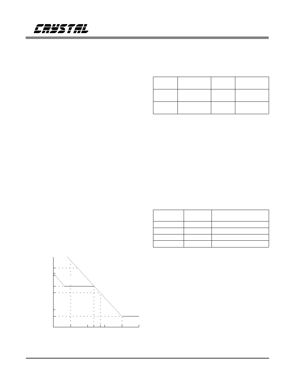
The clock recovery circuit is a second-order
phase locked loop that can tolerate up to 0.4 UI
of jitter from 10 kHz to 100 kHz without gener-
ating errors (Figure 8). The clock and data
recovery circuit is tolerant of long strings of con-
secutive zeros and will successfully recover a
1-in-175 jitter-free line input signal.
Re co vered data at RPOS and RNEG (or
RDATA) is stable and may be sampled using the
recovered clock RCLK. The CLKE input deter-
mines the clock polarity for which output data is
stable and valid as shown in Table 2. When
CLKE is low, RPOS and RNEG (or RDATA) are
valid on the rising edge of RCLK. When CLKE
is high, RPOS and RNEG (or RDATA) are valid
on the falling edge of RCLK.
CLKE
DATA
CLOCK
Clock Edge
for Valid Data
LOW
RPOS, RNEG
or RDATA
RCLK
RCLK
Rising
Rising
HIGH
RPOS, RNEG
or RDATA
RCLK
RCLK
Falling
Falling
Table 2. Recovered Data/Clock Options
JITTER ATTENUATOR
The jitter attenuator can be switched into either
the receive or transmit paths. Alternatively, it can
also be removed from both paths to reduce the
propagation delay.
The location of the attenuators for both channels
is controlled by the ATTEN0 and ATTEN1 pins.
Table 3 shows how these pins are decoded.
The attenuator consists of a 64-bit FIFO, a nar-
row-band monolithic PLL, and control logic.
Signal jitter is absorbed in the FIFO which is de-
signed to neither overflow nor underflow. If
overflow or underflow is imminent, the jitter
transfer function is altered to insure that no bit-
errors occur. Under this condition, jitter gain
may occur and jitter should be attenuated exter-
nally in a frame buffer. The jitter attenuator will
typically tolerate 43 UIs before the overflow/un-
d er f l o w m ec h a n i s m o c cu r s . I f t h e j it ter
attenuator has not had time to "lock" to the aver-
10
1k
10k
1
100
100k
700
.1
1
10
100
.4
28
300
300
PEAK-TO-PEAK
JITTER
(unit intervals)
JITTER FREQUENCY (Hz)
CS61583
Performance
138
AT&T 62411
(1990 Version)
Figure 8. Minimum Input Jitter Tolerance of Receiver
(Clock Recovery Circuit and Jitter Attenuator)
ATTEN1
ATTEN0
Location of
Jitter Attenuator
0
0
Receiver
0
1
Disabled
1
0
Transmitter
1
1
Reserved
Table 3. Jitter Attenuation Control
CS61583
12
DS172PP5