4 power supply characteristics, 5 thermal data (100-pin lqfp with exposed pad), 6 digital switching characteristics-reset – Cirrus Logic CS470xx User Manual
Page 13: 6 digital switching characteristics–reset
13
DS787PP9
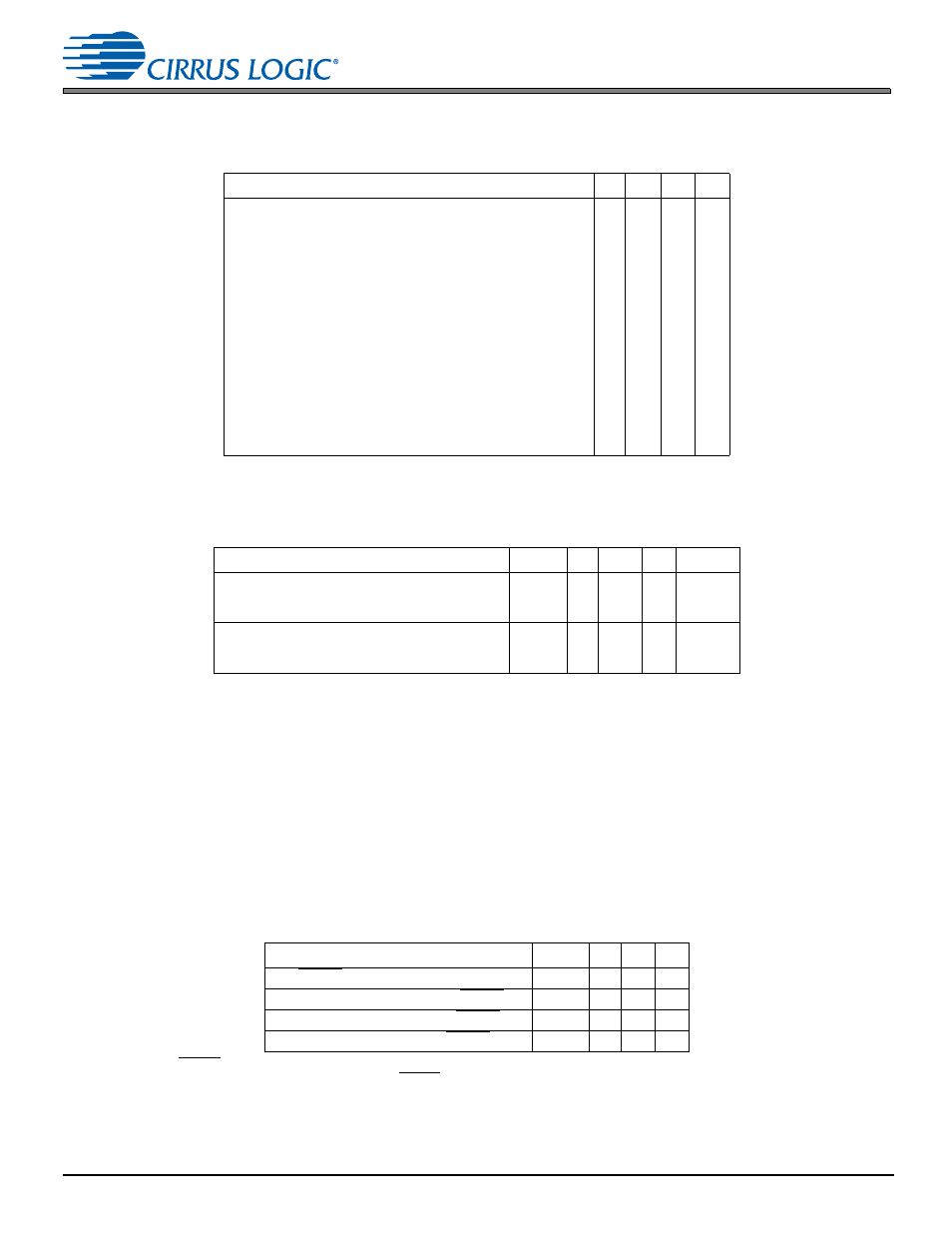
5.4 Power Supply Characteristics
5.4 Power Supply Characteristics
Note:
Measurements performed under operating conditions
1. Dependent on application firmware and DSP clock speed.
5.5 Thermal Data (100-pin LQFP with Exposed Pad)
1. To calculate the die temperature for a given power dissipation:
j
= Ambient temperature + [ (Power Dissipation in Watts) *
ja
]
2. To calculate the case temperature for a given power dissipation:
c
=
j
- [ (Power Dissipation in Watts) *
jt
]
Note:
Two-layer board is specified as a 76 mm X 114 mm, 1.6 mm thick FR-4 material with 1-oz. copper covering 20%
of the top and bottom layers.
Four-layer board is specified as a 76 mm X 114 mm, 1.6 mm thick FR-4 material with 1-oz. copper covering 20% of the
top and bottom layers and 0.5-oz. copper covering 90% of the internal power plane and ground plane layers.
5.6 Digital
Switching
Characteristics–RESET
1. The rising edge of RESET must not occur before the power supplies are stable at the recommended operating values as described in
addition, for the configuration pins to be read correctly, the RESET T
rstl
requirement must be met.
Parameter
Min Typ Max Unit
Operational Power Supply Current:
VDD: Core and I/O operating
1
VDDA: PLL operating current
VDDA: DAC operating current (all 8 channels enabled)
VDDA: ADC operating current (all 4 channels enabled)
VDDIO: With most ports operating
Total Operational Power Dissipation:
Standby Power Supply Current:
VDD: Core and I/O not clocked
VDDA: PLLs halted
VDDA: DAC disabled
VDDA: ADC disabled
VDDIO: All connected I/O pins 3-stated by other ICs in system
Total Standby Power Dissipation:
—
—
—
—
—
—
—
—
—
—
325
16
56
34
27
1025
410
26
40
24
215
1745
—
—
—
—
—
—
—
—
—
—
mA
mA
mA
mA
mA
mW
μA
μA
μA
μA
μA
μW
Parameter
Symbol Min
Typ
Max
Unit
Thermal Resistance (Junction to Ambient)
Two-layer Board
1
Four-layer Board
2
ja
—
—
34
18
—
—
°C/Watt
Thermal Resistance (Junction to Top of Package)
Two-layer Board
1
Four-layer Board
2
jt
—
—
0.54
.28
—
—
°C/Watt
Parameter
Symbol Min Max Unit
RESET minimum pulse width low
1
T
rstl
1
—
s
All bidirectional pins high-Z after RESET low
T
rst2z
—
200
ns
Configuration pins setup before RESET high
T
rstsu
50
—
ns
Configuration pins hold after RESET high
T
rsthld
20
—
ns