5 characteristics and specifications, 1 absolute maximum ratings, 2 recommended operating conditions – Cirrus Logic CS470xx User Manual
Page 12: 3 digital dc characteristics
DS787PP9
12
5 Characteristics and Specifications
5 Characteristics and Specifications
Note:
All data sheet minimum and maximum timing parameters are guaranteed over the rated voltage and temperature.
All data sheet typical parameters are measured under the following conditions: T = 25°C, VDD = 1.8 V, VDDIO =
VDDA = 3.3 V, GND = GNDIO = GNDA = 0 V.
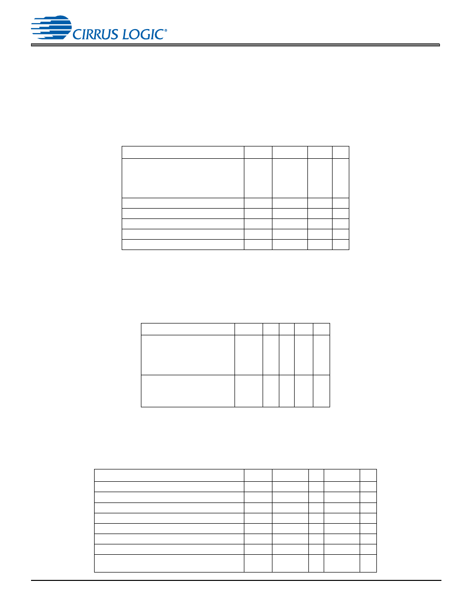
5.1 Absolute Maximum Ratings
(GND = GNDIO = GNDA = 0V; all voltages with respect to 0V)
WARNING:
Operation at or beyond these limits can result in permanent damage to the device. Normal operation is not
guaranteed at these extremes.
5.2 Recommended
Operating
Conditions
(GND = GNDIO = GNDA = 0V; all voltages with respect to 0V)
Note:
It is recommended that the 3.3 V IO supply come up ahead of or simultaneously with the 1.8 V core supply.
5.3 Digital
DC
Characteristics
(Measurements performed under static conditions.)
Parameter
Symbol
Min
Max
Unit
DC power supplies:
Core supply
Analog supply
I/O supply
|VDDA–VDDIO|
VDD
VDDA
VDDIO
–0.3
–0.3
–0.3
—
2.0
3.6
3.6
0.3
V
V
V
V
Input pin current, any pin except supplies I
in
—
±10
mA
Input voltage on PLL_REF_RES
V
filt
–0.3
3.6
V
Input voltage on digital I/O pins
V
inio
–0.3
5.0
V
Analog Input Voltage
V
in
AGND–0.7 VA+0.7
V
Storage temperature
T
stg
–65
150
°C
Parameter
Symbol Min Typ Max Unit
DC power supplies:
Core supply
Analog supply
I/O supply
|VDDA – VDDIO|
VDD
VDDA
VDDIO
1.71
3.13
3.13
1.8
3.3
3.3
0
1.89
3.46
3.46
V
V
V
V
Ambient operating temperature
Commercial—CQZ (147 MHz)
Automotive—DQZ (131 MHz)
Automotive—DQZ (113 MHz)
T
A
0
–40
–40
—
+70
+85
+105
°C
Parameter
Symbol
Min
Typ
Max
Unit
High-level input voltage
V
IH
2.0
—
—
V
Low-level input voltage, except XTI
V
IL
—
—
0.8
V
Low-level input voltage, XTI
V
ILKXTI
—
—
0.6
V
Input Hysteresis
V
hys
—
0.4
—
V
High-level output voltage (I
O
= –2mA), except XTO
V
OH
VDDIO*0.9 —
—
V
Low-level output voltage (I
O
= 2mA), except XTO
V
OL
—
— VDDIO*0.1
V
Input leakage XTI
I
LXTI
—
—
5
μ
A
Input leakage current (all digital pins with internal
pull-up resistors enabled)
I
LEAK
—
—
70
μ
A