Constraint 7: note on frequency and emi, An374 – Cirrus Logic AN374 User Manual
Page 16
AN374
16
AN374REV2
The following are disclaimers for this analysis:
a. This analysis works better for a non-isolated design. For isolated flyback designs, the size may be deter-
mined by safety requirements for either triple insulated wire or margin tape spacing. As a result,
increased peak current may or may not translate into the size of the inductor easily.
b. The explanation above shows a qualitative trend in understanding the tradeoffs of having power deliv-
ered to two strings unevenly. It is understood that it is not possible to determine a true analogy since the
reflected voltage and frequency vary over the two modes of operation in the CS1630/31. This compar-
ison should only be viewed from a qualitative understanding of the system.
5. When considering efficiency, if the power delivered to the load in the two modes is significantly different,
then the frequency of operation of switching frequency F
sw1
and F
sw2
will be significantly different because
the converter operates in CRM at full brightness.
The converter will switch at a very high frequency while converting very little power. The power converter’s
efficiency is low, however the power is transferred at two different frequencies and some amount of
spreading effects of the spectral energy can be observed. This can potentially be favorable from an EMI
perspective.
Step 4) Analyze system tradeoffs for efficiency when using a flyback topology
In a parallel configuration, the turns ratio will be higher for a given reflected voltage, so the leakage inductance
will also be higher. As a result, the peak voltage on the drain of the flyback MOSFET must be taken into
account. Since the effective output voltage is smaller, the synchronizer diode drop amounts to a much bigger
efficiency penalty as opposed to the parallel design case.
In a series design, the leakage inductance will be smaller for the same reflected voltage. The maximum voltage
on the rectifier diode is given by V
IN
/ N + V
OVP
. The diode must be a higher voltage rated diode, which
increases cost and may impact efficiency, depending on the reflected voltage.
In a flyback topology, it is difficult to predict the diode losses prior to the development of a system, since diode
losses vary significantly with junction temperature. This step is meant to serve as an added consideration when
choosing a certain load configuration.
Step 5) Analyze system tradeoffs for efficiency when using a buck topology
The minimum voltage rating for the power diode is greater than 250V for the CS1630 and greater than 450V
for the CS1631. In order to guarantee optimum output current regulation in a buck converter, it is desirable to
have a duty cycle of at least 10%, and any duty cycle above 15% is considered optimal for the buck converter.
In a parallel configuration, the effective output voltage is lower, and the diode losses higher. The duty cycle is
smaller, since the effective output voltage is smaller. In a series configuration, the diode losses are lower, since
the diode drop is still set by the boost voltage V
BST
and not the output voltage.
Constraint 7: Note on Frequency and EMI
The frequency of the double pulse is dependent on the ratio of the power delivered in each mode. Both strings
having different power levels provides natural spreading of the spectrum for EMI. However, it decreases the
magnetic utilization of the core.
The following are the hard constraints on the frequency of operation:
1. Maximum switching frequency cannot exceed 200kHz.
2. Minimum switching frequency cannot be lower than the value programmed in the OTP register TTMAX at
Address 38.
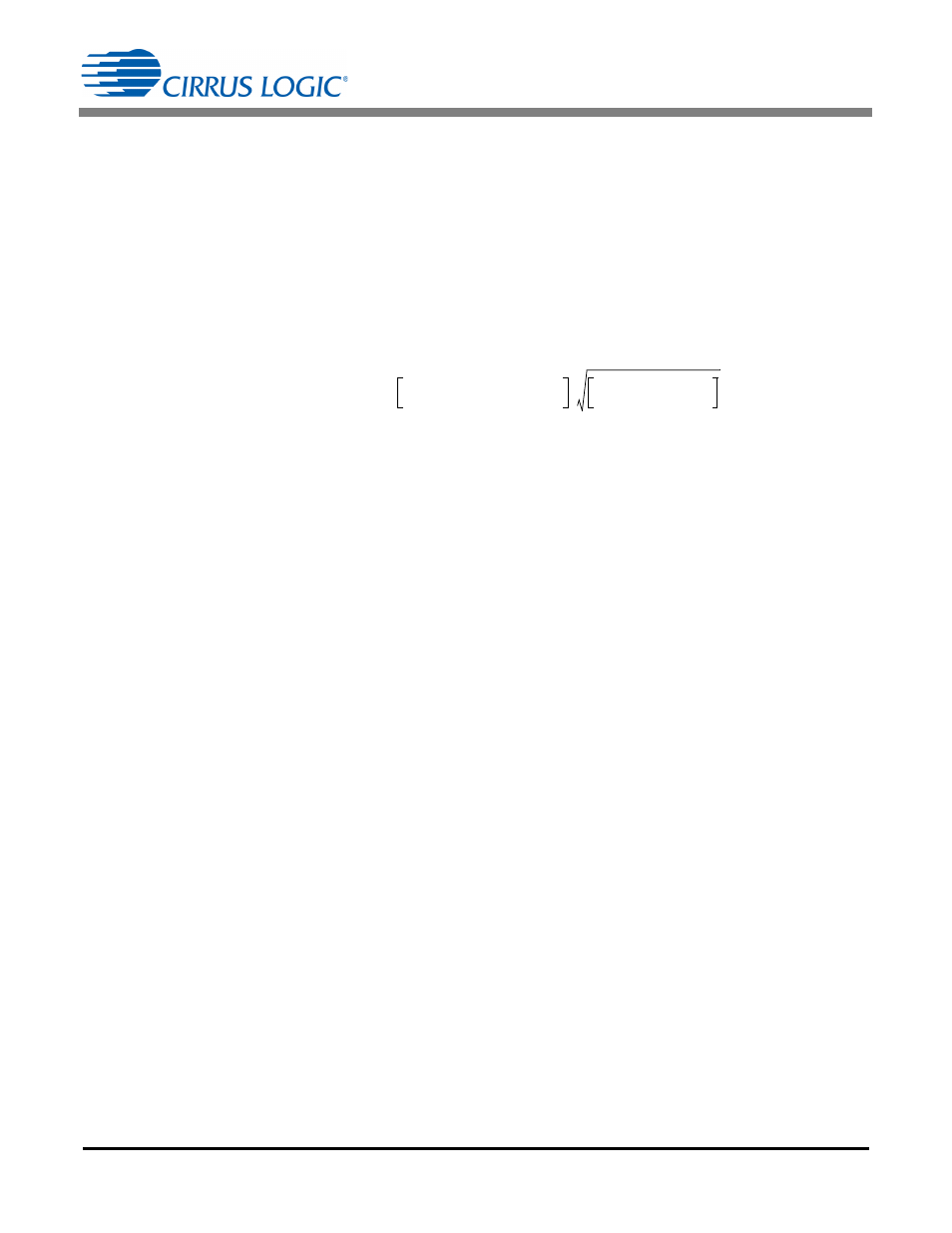
F
SW2
F
SW1
V
BST
N V
MODE1
+
V
BST
N V
MODE2
+
----------------------------------------------------------
I
MODE1
V
MODE2
I
MODE2
V
MODE1
------------------------------------------
=
[Eq. 14]