An374, Figure 4c. flyback series output model – Cirrus Logic AN374 User Manual
Page 12
AN374
12
AN374REV2
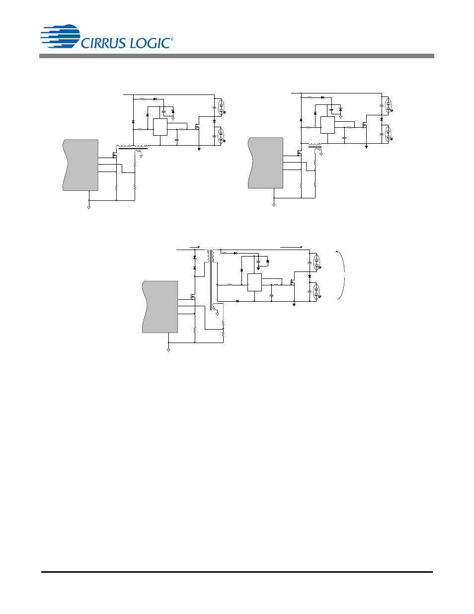
Flyback topology is enabled by setting bit S2CONFIG to ‘1’ in register Config12 at address 44. A flyback
topology is selected as a design guide example in application note AN368 so bit S2CONFIG is set to ‘1’. The
flyback transformer input-to-output voltage ratio is used to determine the duty cycle and minimum turn on time
T1 for the power FET. Buck topology is enabled by setting bit S2CONFIG to ‘0’ in register Config12 at address
44. If a buck topology is selected, the buck inductor is configured using bits BUCK[3:0] in register Config10 at
address 42. Set bits BUCK[3:0] to ‘0’ or ‘1’ for a normal buck topology. Tapped buck topology is enabled by
setting bit S2CONFIG to ‘0’ in register Config12 at address 44 and by setting bits BUCK[3:0] in register
Config10 at address 42 to the required value N, where N equals the turns ratio between primary and secondary
windings.
Figure 4a. Tapped Buck Series Output Model
Figure 4b. Buck Series Output Model
R22
R21
R23
Q5
L3
D3
CS1630 /31
FBAUX
GND
13
GD
FBSENSE
15
12
11
V
B S T
R3
D9
U2
C10
C8
C15
D11
D
GND
_
Q
V CC
R12
D10
Q3
R2
C14
Channel 1 LED
(White)
Channel 2 LED
(Red)
GND
IGND
D9
R22
R21
R23
Q4
L3
CS1630 /31
FBAUX
GND
13
GD
FBSENSE
15
12
11
D3
V
B S T
R25
D9
U2
C13
C15
C16
D11
D
GND
_
Q
V CC
R26
D10
Q5
R27
C14
Z3
Channel 1 LED
(White)
Channel 2 LED
(Red)
GND
IGND
Figure 4c. Flyback Series Output Model
D2
R22
Z3
R21
R23
Q5
CS1630 /31
FBAUX
GND
13
GD
FBSENSE
15
12
11
TX1
V
B S T
R3
D6
U2
C10
C8
C15
D5
D
GND
_
Q
V CC
D15
R12
D10
Q 3
R2
C16
Channel 1 LED
(White)
Channel 2 LED
(Red)
GND
IGND
I
MODE x
I
P RI
V
MODE x
D9