3 pin assignments for x16 lane widths, Pin assignments for x16 lane widths – Teledyne LeCroy PCI Express 2.0 Mid-Bus Probe Ver.2.40 User Manual
Page 16
Teledyne LeCroy
PCIe 2.0 Mid-Bus Probe Installation Guide
Version 2.4
12
In the pinout tables that follow, the following variations may be applied:
• The designation of upstream and downstream may be reversed as long as it is reversed for every
lane (all upstream connections on the left and all downstream on the right may be swapped)
• Lane ordering may be reversed if done as a whole such that probe lanes 0, 1, 2, 3, 4, 5, 6, 7
connect to physical lanes 7, 6, 5, 4, 3, 2, 1, 0. Note that the Summit T2-16 analyzer provides the
flexibility to reorder lanes regardless of the order in which they are physically connected (lane
swizzling).
• Each differential signal pair may have the D+ and D- assignment reversed.
• If the Gen2 footprint is used, an additional ground pin is present above Pin1 and below Pin48 (not
shown in tables).
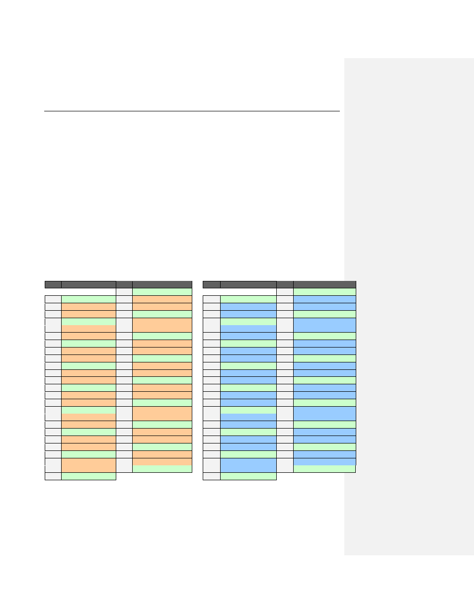
4.3 Pin Assignments for x16 Lane Widths
For x16 lane widths, two full-size headers are required. The diagrams below show the recommended pin
assignments for x16 configurations (keep in mind that any of modifications mentioned in Section 4.2 can
be applied, and in addition the lane swizzling feature of the Summit T3-16 and T2-16 systems noted in
Section 4.2).
x16 (in Two Unidirectional Footprints) Mid-Bus Probe Pinout
on two Full-size Headers (Summit only)
Pin
Signal Name
Pin
Signal Name
G1
GND (Gen2 only)
A2
GND
A1
C0p- Downstream
A4
C1p- Downstream
A3
C0n- Downstream
A6
C1n- Downstream
A5
GND
A8
GND
A7
C2p- Downstream
A10
C3p- Downstream
A9
C2n- Downstream
A12
C3n- Downstream
A11
GND
A14
GND
A13
C4p- Downstream
A16
C5p- Downstream
A15
C4n- Downstream
A18
C5n- Downstream
A17
GND
A20
GND
A19
C6p- Downstream
A22
C7p- Downstream
A21
C6n- Downstream
A24
C7n- Downstream
A23
GND
A26
GND
A25
C8p- Downstream
A28
C9p- Downstream
A27
C8n- Downstream
A30
C9n- Downstream
A29
GND
A32
GND
A31
C10p- Downstream
A34 C11p- Downstream A33
C10n- Downstream
A36 C11n- Downstream A35
GND
A38
GND
A37
C12p- Downstream
A40 C13p- Downstream A39
C12n- Downstream
A42 C13n- Downstream A41
GND
A44
GND
A43
C14p- Downstream
A46 C15p- Downstream A45
C14n- Downstream
A48 C15n- Downstream A47
GND
G2
GND (Gen2 only)
Pin
Signal Name
Pin
Signal Name
G1
GND (Gen2 only)
B2
GND
B1
C0p- Upstream
B4
C1p- Upstream
B3
C0n- Upstream
B6
C1n- Upstream
B5
GND
B8
GND
B7
C2p- Upstream
B10
C3p- Upstream
B9
C2n- Upstream
B12
C3n- Upstream
B11
GND
B14
GND
B13
C4p- Upstream
B16
C5p- Upstream
B15
C4n- Upstream
B18
C5n- Upstream
B17
GND
B20
GND
B19
C6p- Upstream
B22
C7p- Upstream
B21
C6n- Upstream
B24
C7n- Upstream
B23
GND
B26
GND
B25
C8p- Upstream
B28
C9p- Upstream
B27
C8n- Upstream
B30
C9n- Upstream
B29
GND
B32
GND
B31
C10p- Upstream
B34
C11p- Upstream
B33
C10n- Upstream
B36
C11n- Upstream
B35
GND
B38
GND
B37
C12p- Upstream
B40
C13p- Upstream
B39
C12n- Upstream
B42
C13n- Upstream
B41
GND
B44
GND
B43
C14p- Upstream
B46
C15p- Upstream
B45
C14n- Upstream
B48
C15n- Upstream
B47
GND
G2
GND (Gen2 only)
A unidirectional x16 configuration can be implemented using one full-size header (utilizing the pinout
diagram on the right – for upstream traffic – or the diagram on the left – for downstream traffic).