6 block diagram – 3744a receiver module, 7 3744a-rx receiver compression, noise floor, Composite receiver dut – Atec Anritsu-ME7838A User Manual
Page 20

20
PN: 11410-00593 Rev. D
ME7838A BB/mm-Wave VNA TDS
Waveguide Band Specifications and Performance
VectorStar ME7838A BB/mm-Wave VNA
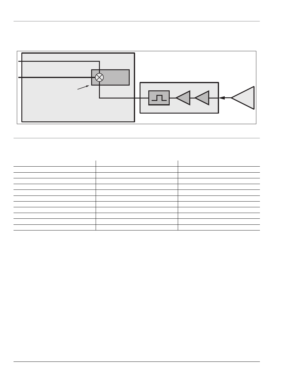
3.6 Block Diagram – 3744A Receiver Module
As with all cold source method noise figure measurements, the output of the DUT is first sent to an external composite receiver for
pre-amplification. This ensures that the system noise figure is minimized for optimum measurement accuracy. The Anritsu Noise Figure
Uncertainty Calculator (available on the website at
an be used to determine optimum preamplifier gain needed for the
desired measurement uncertainty.
Composite Receiver
DUT
30 GHz - 125 GHz
3744A-Rx 30 GHz - 125 GHz Receiver Module
Nonlinear
Transmission Line
GaAs Sampler
LO
Test IF
3744A-Rx Block Diagram
3.7 3744A-Rx Receiver Compression, Noise Floor
Receiver Compression Point is defined as the port power level beyond which the response may be compressed more than 0.2 dB relative to the
normalization level. 10 Hz IF bandwidth is used to remove trace noise effects. All typical.
Noise Floor is relative to the receiver power calibration performed at –10 dBm. Typical.
Frequency
Receiver Compression (dBm)
a
a. At the 3744A-Rx test port.
54 to 60 GHz
0
-122
60 to 67 GHz
0
-117
67 to 80 GHz
0
-120
80 to 85 GHz
0
-123
85 to 90 GHz
0
-121
90 to 95 GHz
0
-121
95 to 105 GHz
0
-117
105 to 110 GHz
0
-122
110 to 120 GHz
-5
-120
120 to 125 GHz
-5
-117
Noise Floor (dBm)
b
b. Excludes localized spurious responses and crosstalk.
30 to 54 GHz
0
-124
