20a digital microdlynx, Non-isolated dc-dc power modules, Data sheet – GE Industrial Solutions 20A Digital MicroDLynx User Manual
Page 23
GE
Data Sheet
20A Digital MicroDLynx
TM
: Non-Isolated DC-DC Power Modules
3Vdc –14.4Vdc input; 0.45Vdc to 5.5Vdc output; 20A Output Current
April 24, 2013
©2012 General Electric Company. All rights reserved.
Page 23
T
IND
, it may be approximated by an estimate of the module
temperature.
Measuring Output Voltage Using the PMBus
The module can provide output voltage information using
the READ_VOUT command. The command returns two bytes
of data all representing the mantissa while the exponent is
fixed at -10 (decimal).
During manufacture of the module, offset and gain
correction values are written into the non-volatile memory
of the module. The command VOUT_CAL_OFFSET can be
used to read and/or write the offset (two bytes consisting of
a 16-bit mantissa in two’s complement format) while the
exponent is always fixed at -10 (decimal). The allowed range
for this offset correction is -125 to 124mV. The command
VOUT_CAL_GAIN can be used to read and/or write the gain
correction - two bytes consisting of a five-bit exponent (fixed
at -8) and a 11-bit mantissa. The range of this correction
factor is -0.125 to +0.121, with a resolution of 0.004. The
corrected output voltage reading is then given by:
OFFSET
CAL
VOUT
GAIN
CAL
VOUT
Initial
V
Final
V
OUT
OUT
_
_
)]
_
_
1
(
)
(
[
)
(
.
Measuring Input Voltage Using the PMBus
The module can provide output voltage information using
the READ_VIN command. The command returns two bytes
of data in the linear format. The upper five bits [7:3] of the
high data form the two’s complement representation of the
exponent which is fixed at –5 (decimal). The remaining 11
bits are used for two’s complement representation of the
mantissa, with the 11
th
bit fixed at zero since only positive
numbers are valid.
During module manufacture, offset and gain correction
values are written into the non-volatile memory of the
module. The command VIN_CAL_OFFSET can be used to
read and/or write the offset - two bytes consisting of a five-
bit exponent (fixed at -5) and a11-bit mantissa in two’s
complement format. The allowed range for this offset
correction is -2to 1.968V, and the resolution is 32mV. The
command VIN_CAL_GAIN can be used to read and/or write
the gain correction - two bytes consisting of a five-bit
exponent (fixed at -8) and a 11-bit mantissa. The range of
this correction factor is -0.125 to +0.121, with a resolution of
0.004. The corrected output voltage reading is then given by:
OFFSET
CAL
VIN
GAIN
CAL
VIN
Initial
V
Final
V
IN
IN
_
_
)]
_
_
1
(
)
(
[
)
(
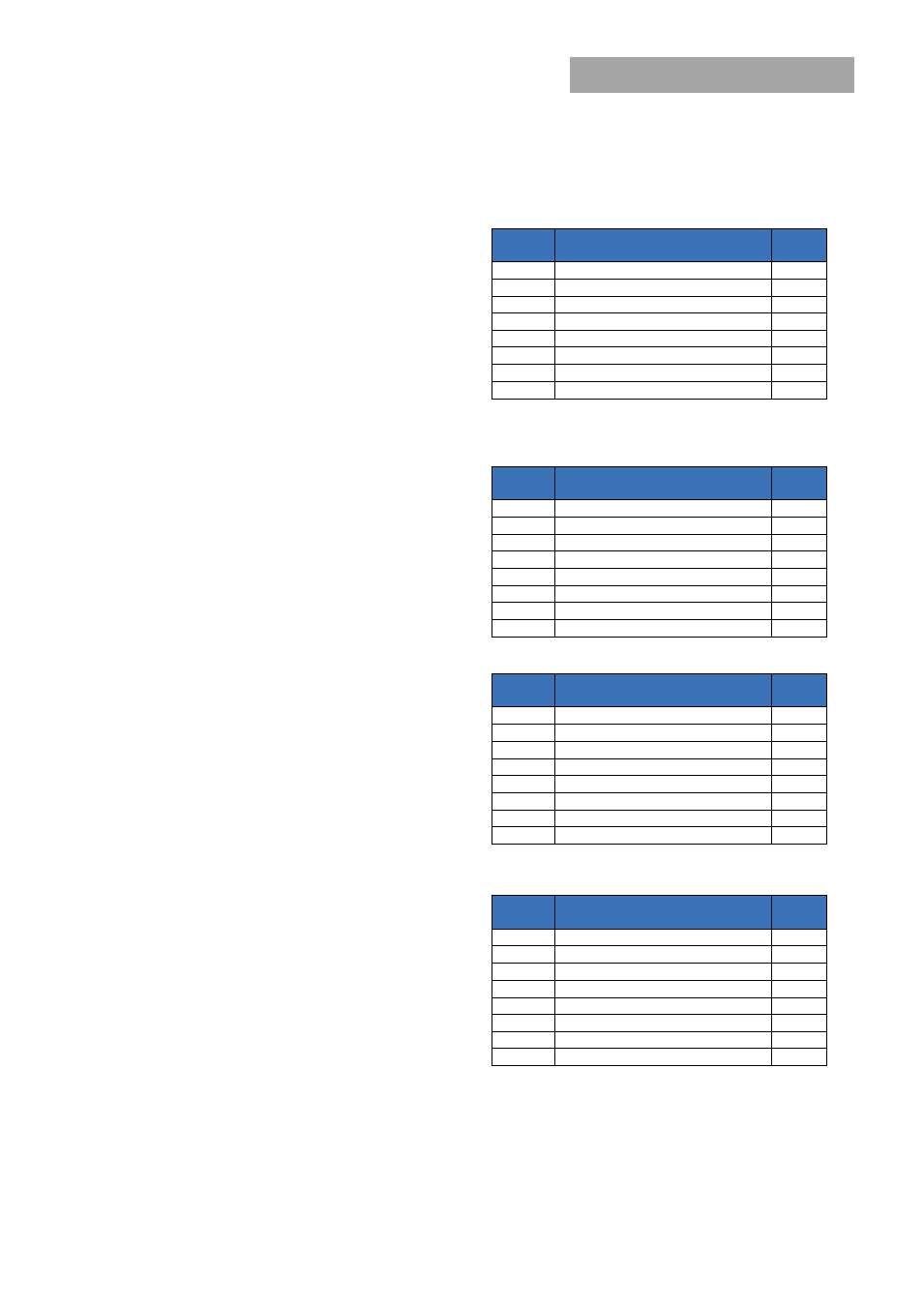
Reading the Status of the Module using the PMBus
The module supports a number of status information
commands implemented in PMBus. However, not all
features are supported in these commands. A 1 in the bit
position indicates the fault that is flagged.
STATUS_BYTE : Returns one byte of information with a
summary of the most critical device faults.
Bit
Position
Flag
Default
Value
7
X
0
6
OFF
0
5
VOUT Overvoltage
0
4
IOUT Overcurrent
0
3
VIN Undervoltage
0
2
Temperature
0
1
CML (Comm. Memory Fault)
0
0
None of the above
0
STATUS_WORD: Returns two bytes of information with a
summary of the module’s fault/warning conditions.
Low Byte
Bit
Position
Flag
Default
Value
7
X
0
6
OFF
0
5
VOUT Overvoltage
0
4
IOUT Overcurrent
0
3
VIN Undervoltage
0
2
Temperature
0
1
CML (Comm. Memory Fault)
0
0
None of the above
0
High Byte
Bit
Position
Flag
Default
Value
7
VOUT fault or warning
0
6
IOUT fault or warning
0
5
X
0
4
X
0
3
POWER_GOOD# (is negated)
0
2
X
0
1
X
0
0
X
0
STATUS_VOUT : Returns one byte of information relating to
the status of the module’s output voltage related faults.
Bit
Position
Flag
Default
Value
7
VOUT OV Fault
0
6
X
0
5
X
0
4
VOUT UV Fault
0
3
X
0
2
X
0
1
X
0
0
X
0