Pim400 series; atca board power input modules, Data sheet, Digital feature descriptions – GE Industrial Solutions PIM400 Series User Manual
Page 16
GE
Data Sheet
PIM400 Series; ATCA Board Power Input Modules
-36 to -75 Vdc; 400W/10A
June 20, 2013
©2013 General Electric Company. All rights reserved.
Page 16
Digital Feature Descriptions
Full featured modules are available with I
2
C Digital Interface
(Option -K).
Modules with I
2
C capability monitor up to five analog
parameters and six status bits identified below in Tables 1and 2
respectively.
Modules with I
2
C Option Features:
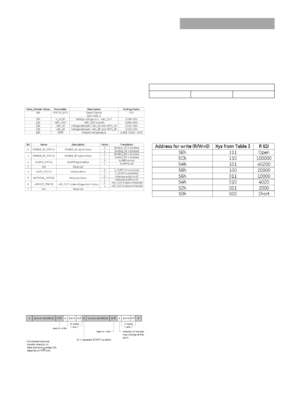
Table 1: Internal register memory map
Table 2: Digital signals
Note: Bit 0=LSB, Bit 7=MSB
I
2
C Command Structure:
The I
2
C is a 2-wire interface supporting multiple devices and
masters on a single bus. The connected devices can only pull
the bus wires low and they never drive the bus high. The bus
wires should be externally connected to a positive supply
voltage via a pull-up resistor. When the bus is idle, both DAT
and CLK are high.
Each device on the I
2
C bus is recognized by a unique address
stored in that device. Devices can be classified as masters or
slaves when performing data transfers. A master is a device
which initiates a data transfer on the bus and generates clock
signals to permit that transfer. At the same time, any device
addressed is considered slave. The PIM400 always acts as a
slave.
In PIM400 module, I
2
C interface is used for reporting critical
parameters like input voltage, output current, holdup capacitor
voltage and temperature data. The read protocol is shown in
the Fig 20 below.
Fig 20: Typical I
2
C Read protocol
Address Structure:
7 bit Address + R/W bit
Four bits are fixed (0101), three bits (xyz) are variable, and the
least-significant bit is the read/write bit.
8 bit Address
0101
xyz*
R/W
Table 3: Address structure
Address Selection:
The three bits (xyz) of the address are set with a single external
resistor from the ADD (pin10) to LOGIC_GND (pin 13). The 8
possible addresses are shown in Table 4 with the respective
resistance values.
Table 4: I
2
C Addressing