Pim400 series; atca board power input modules, Data sheet, Feature descriptions – GE Industrial Solutions PIM400 Series User Manual
Page 12: Design considerations, Inrush current control / hot plug functionality
GE
Data Sheet
PIM400 Series; ATCA Board Power Input Modules
-36 to -75 Vdc; 400W/10A
June 20, 2013
©2013 General Electric Company. All rights reserved.
Page 12
Feature Descriptions
Introduction
The PIM400X module is designed to support the Advanced
Telecommunications Computing Architecture (ATCA) power
entry distribution requirements for the Front Board / Blade per
the PICMG 3.0 specifications.
The PICMG 3.0 specification defines the Mechanical, Shelf
Management Interface, Power Distribution, Thermal, Data I/O
and Regulatory requirements for the next generation of
modular telecom architecture platform for use in Central Office
telecom environments.
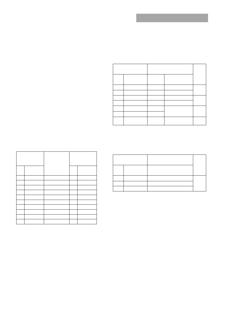
Input Pin Connections
The ATCA board is specified to accept up to a maximum of
400W of input power via dual, redundant -48Vdc Feeds
through the Zone 1 (Power and Management) connector,
designated P10.
The power connector provides board to backplane
engagement via pins of varying lengths. Please consult the
PICMG 3.0 specifications for details.
The following are the design considerations of the input pin
connections of the PIM400X to the ATCA power connector.
From
ATCA
(P10 Connector)
Connection
Requirement
To
PIM400X
Pin
#
Pin
Designation
Pin
#
Signal
Designation
33
-48V_A
Via Fuse(F3)
1
-48V_AF
34
-48V_B
Via Fuse(F4)
2
-48V_BF
28
VRTN_A
Via Fuse(F1)
3
VRTN_AF
29
VRTN_B
Via Fuse(F2)
4
VRTN_BF
30
EARLY_A
Via Resistor(R1) *
-48V_A
31
EARLY_B
Via Resistor(R2) *
-48V_B
32
ENABLE_A
Via Fuse(F5)
5
ENABLE_AF
27
ENABLE_B
Via Fuse(F6)
6
ENABLE_BF
25
SHELF_GND
Direct
7
SHELF_GND
26
LOGIC_GND
Direct
11
LOGIC_GND
* Pre-charge resistors
The first pins to mate in the ATCA power connector are the
EARLY_A, EARLY_B, the two grounds (LOGIC_GND, SHELF_GND)
and the two returns (VRTN_A, VRTN_B); followed by staggered
connections of -48V_A and -48V_B power Feeds. The last pins
to engage are the two short pins, ENABLE_A & ENABLE_B. The
ATCA backplane connects the ENABLE_A to VRTN_A, ENABLE_B
to VRTN_B, EARLY_A to -48V_A and EARLY_B to -48V_B.
EARLY_A & EARLY_B Connections: During hot insertion of the
ATCA board, the Inrush Control circuit limits the surge current
to the C_FLTR capacitor. However, due to the presence of a
small amount of internal EMI filter capacitance (located before
the Inrush Control circuit), it is recommended that Precharge
resistors, R1 & R2 (100 Ohms, with appropriate surge capability)
be connected as shown in the Typical Application circuit.
Output Pin Connections (Standard Module: PIM400Z)
The output pin connections of the PIM400X to the system board
are described below:
From
PIM400X
To
ATCA Front Board
Notes
Pin
#
Pin
Designation
Terminal
Component
15
-48V_OUT
Vin(-)
DC/DC Converter
(1)
17
VRTN_OUT
Vin(+)
DC/DC Converter
18
V_HLDP
+ve
Holdup Capacitor
(2)
16
TRIM_HLDP
RTrim
Holdup Capacitor
8
+5V0
Management
Power
(3)
9
+3V3
14
ALARM
R
pull-up
IPM/System
Controller
(4)
Additional Output Pin Connections (Modules with
optional I
2
C Digital Interface: Option - K)
The following additional output pins of the PIM400KZ available
for I
2
C Digital Interface to the IMP/System Controller are
defined below:
From
PIM400KZ
To
ATCA Front Board
Notes
Pin
#
Pin
Designation
IPM/System Controller I2C
Interface
10
ADD
I2C Address w.r.t. LOGIC_GND
(5)
11
DAT
I2C Data w.r.t. LOGIC_GND
12
CLK
I2C Clock w.r.t. LOGIC_GND
Inrush Current Control / Hot Plug Functionality
The module provides inrush current control / hot plug
capability. The peak value of the inrush current and the
duration complies with the PICMG 3.0’s Inrush Transient
specifications. The specifications shall be met with the external
C_HLDP and C_FLTR capacitances as specified in the previous
sections.
The unique design of the module where the large energy
storage capacitors are segregated from the input filter
capacitors allows the module to meet the stringent PICMG’s
inrush transient specifications with minimal energy storage
capacitors.
Design Considerations
-48V Main Output Bus:
(Signal Names: -48V_OUT & VRTN_OUT)
This is the main -48V output bus that provides the payload
power to the downstream (one or more) DC/DC converters. The