1 qe bit – Rainbow Electronics AT45DQ321 User Manual
Page 35
35
AT45DQ321 [ADVANCE DATASHEET]
DS-45DQ321-031–DFLASH–12/2012
Figure 9-1. Configuration Register Format
Note:
1. Only bit seven of the Configuration Register will be modified when using the Quad Enable/Disable
commands.
9.5.1
QE Bit
The QE bit is used to control whether the Quad-input Buffer 1 Write or Buffer 2 Write and the Quad-output Read Array
commands are enabled or disabled. When the QE bit is in the Logical 1 state, the Quad-input Buffer Write and Quad-
output Read Array commands are enabled and will be recognized by the device. In addition, the WP and RESET
functions are disabled and the WP and RESET pins themselves operate as a bidirectional input/output pins (WP is I/O
2
and RESET is I/O
3
).
When the QE bit is in the Logical 0 state, the Quad-Input Buffer Write and Quad-output Read Array commands are
disabled and will not be recognized by the device as valid commands and the WP and RESET pins function as normal
control pins. The WP and RESET pins should be externally pulled-high to avoid erroneous or unwanted device operation.
The Reset command has no effect on the QE bit. The QE bit defaults to the Logical 0 state when devices are initially
shipped from Adesto.
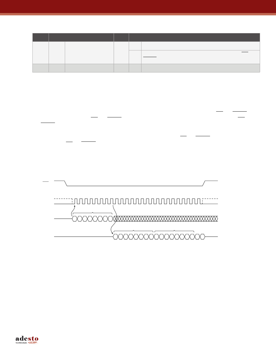
Figure 9-2. Read Configuration Register
Bit
Name
Type
Description
7
QE
Quad Enable
R/W
0
Quad-input/output commands and operation disabled.
1
Quad-input/output commands and operation enabled. (WP and
RESET disabled)
6:0
RES
Reserved for Future Use
R
0
Reserved for future use.
SO
SI
SCK
CS
MSB
2
3
1
0
0
0
1
1
1
1
1
1
6
7
5
4
10 11
9
8
12
21 22
17
20
19
18
15 16
13 14
23 24
Opcode
MSB
MSB
X
X
X
X
X
X
D
X
X
D
MSB
X
X
X
X
X
X
X
D
Configuration
Register Out
Configuration
Register Out
High-impedance