3 read sector protection register – Rainbow Electronics AT45DQ321 User Manual
Page 25
25
AT45DQ321 [ADVANCE DATASHEET]
DS-45DQ321-031–DFLASH–12/2012
clocked into a byte location of the Sector Protection Register, then the protection status of the sector corresponding to
that byte location cannot be guaranteed.
Example:
If a value of 17h is clocked into byte location 2 of the Sector Protection Register, then the protection status
of Sector 2 cannot be guaranteed.
The Sector Protection Register can be reprogrammed while the sector protection is enabled or disabled. Being able to
reprogram the Sector Protection Register with the sector protection enabled allows the user to temporarily disable the
sector protection to an individual sector rather than disabling sector protection completely.
The Program Sector Protection Register command utilizes Buffer 1 for processing. Therefore, the contents of Buffer 1
will be altered from its previous state when this command is issued.
Table 7-7.
Program Sector Protection Register Command
Figure 7-5. Program Sector Protection Register
7.3.3
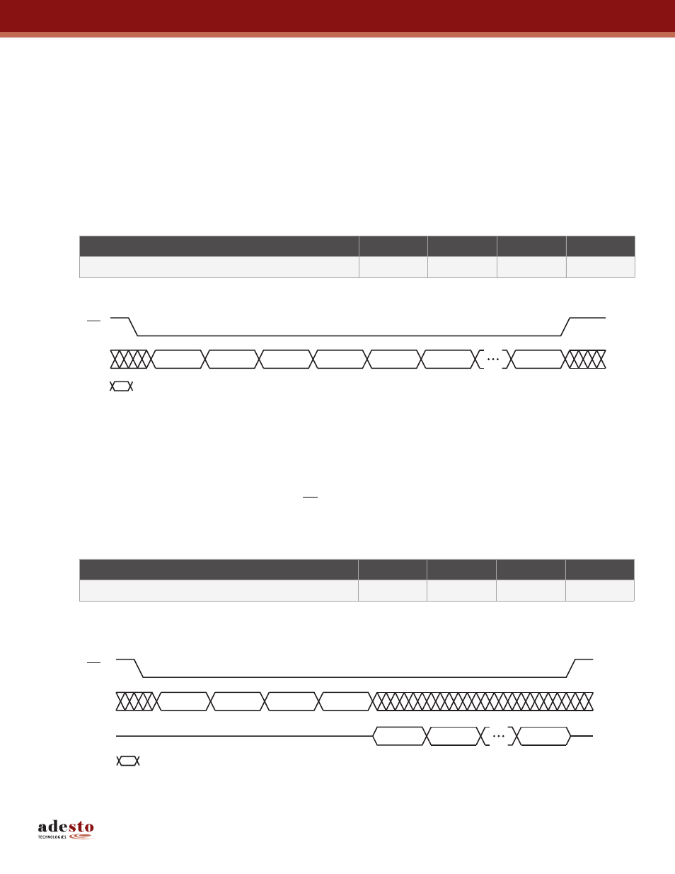
Read Sector Protection Register
To read the Sector Protection Register, an opcode of 32h and three dummy bytes must be clocked into the device. After
the last bit of the opcode and dummy bytes have been clocked in, any additional clock pulses on the SCK pin will result
in the Sector Protection Register contents being output on the SO pin. The first byte (byte location 0) corresponds to
Sector 0 (0a and 0b), the second byte corresponds to Sector 1, and the last byte (byte location 63) corresponds to Sector
63. Once the last byte of the Sector Protection Register has been clocked out, any additional clock pulses will result in
undefined data being output on the SO pin. The CS pin must be deasserted to terminate the Read Sector Protection
Register operation and put the output into a high-impedance state.
Table 7-8.
Read Sector Protection Register Command
Note:
1. XX = Dummy byte
Figure 7-6. Read Sector Protection Register
Command
Byte 1
Byte 2
Byte 3
Byte 4
Program Sector Protection Register
3Dh
2Ah
7Fh
FCh
Data Byte
n
3Dh
2Ah
7Fh
FCh
Data Byte
n + 1
Data Byte
n + 63
CS
Each transition represents eight bits
SI
Command
Byte 1
Byte 2
Byte 3
Byte 4
Read Sector Protection Register
32h
XXh
XXh
XXh
32h
XX
XX
XX
Data
n
Data
n + 1
CS
Data
n + 63
SI
SO
Each transition represents eight bits