Rainbow Electronics AT45DQ321 User Manual
Page 3
3
AT45DQ321 [ADVANCE DATASHEET]
DS-45DQ321-031–DFLASH–12/2012
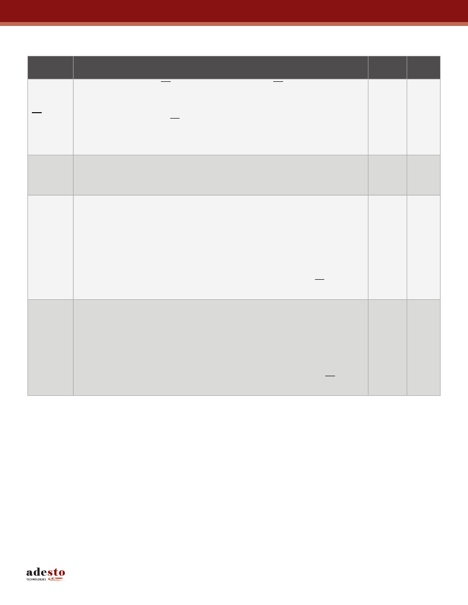
Table 1-1.
Pin Configurations
Symbol
Name and Function
Asserted
State
Type
CS
Chip Select: Asserting the CS pin selects the device. When the CS pin is deasserted, the
device will be deselected and normally be placed in the standby mode (not Deep Power-Down
mode) and the output pin (SO) will be in a high-impedance state. When the device is
deselected, data will not be accepted on the input pin (SI).
A high-to-low transition on the CS pin is required to start an operation and a low-to-high
transition is required to end an operation. When ending an internally self-timed operation such
as a program or erase cycle, the device will not enter the standby mode until the completion of
the operation.
Low
Input
SCK
Serial Clock: This pin is used to provide a clock to the device and is used to control the flow of
data to and from the device. Command, address, and input data present on the SI pin is
always latched on the rising edge of SCK, while output data on the SO pin is always clocked
out on the falling edge of SCK.
—
Input
SI (I/O
0
)
Serial Input (I/O
0
): The SI pin is used to shift data into the device. The SI pin is used for all
data input including command and address sequences. Data on the SI pin is always latched on
the rising edge of SCK.
With the Dual-output and Quad-output Read Array commands, the SI pin becomes an output
pin (I/O
0
) and, along with other pins, allows two bits (on I/O
1-0
) or four bits (on I/O
3-0
) of data to
be clocked out on every falling edge of SCK. To maintain consistency with SPI nomenclature,
the SI (I/O
0
) pin will be referenced as SI throughout the document with exception to sections
dealing with the Dual-output and Quad-output Read Array commands in which it will be
referenced as I/O
0
.
Data present on the SI pin will be ignored whenever the device is deselected (CS is
deasserted).
—
Input/
Output
SO (I/O
1
)
Serial Output (I/O
1
): The SO pin is used to shift data out from the device. Data on the SO pin
is always clocked out on the falling edge of SCK.
With the Dual-output and Quad-output Read Array commands, the SO pin is used as an output
pin (I/O
1
) in conjunction with other pins to allow two bits (on I/O
1-0
) or four bits (on I/O
3-0
) of data
to be clocked out on every falling edge of SCK. To maintain consistency with SPI
nomenclature, the SO (I/O
1
) pin will be referenced as SO throughout the document with
exception to sections dealing with the Dual-output and Quad-output Read Array commands in
which it will be referenced as I/O
1
.
The SO pin will be in a high-impedance state whenever the device is deselected (CS is
deasserted).
—
Input/
Output