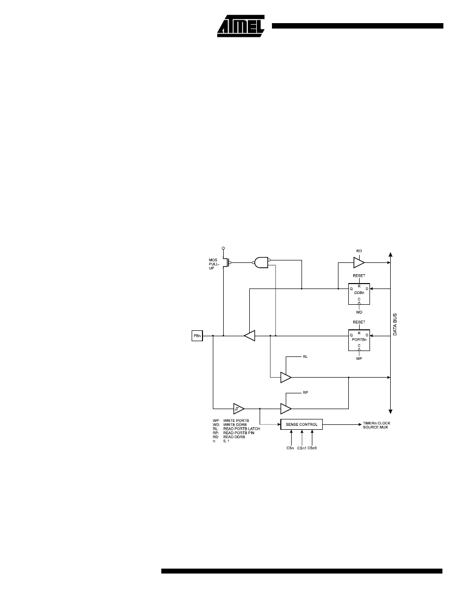
Port b schematics – Rainbow Electronics AT90LS8535 User Manual
Page 80

80
AT90S/LS8535
1041H–11/01
allows analog signals that are close to V
CC
/2 to be present during power-down without
causing excessive power consumption.
• AIN0 – Port B, Bit 2
AIN0, Analog Comparator Positive Input. When configured as an input (DDB2 is cleared
[zero]) and with the internal MOS pull-up resistor switched off (PB2 is cleared [zero]),
this pin also serves as the positive input of the on-chip Analog Comparator. During
Power-down mode, the Schmitt trigger of the digital input is disconnected. This allows
analog signals that are close to V
CC
/2 to be present during power-down without causing
excessive power consumption.
• T1 – Port B, Bit 1
T1, Timer/Counter1 counter source. See the timer description for further details.
• T0 – Port B, Bit 0
T0: Timer/Counter0 counter source. See the timer description for further details.
Port B Schematics
Note that all port pins are synchronized. The synchronization latches are, however, not
shown in the figures.
Figure 52. Port B Schematic Diagram (Pins PB0 and PB1)
2
