Ss pin functionality, Data modes – Rainbow Electronics AT90LS8535 User Manual
Page 56

56
AT90S/LS8535
1041H–11/01
SS Pin Functionality
When the SPI is configured as a master (MSTR in SPCR is set), the user can determine
the direction of the SS pin. If SS is configured as an output, the pin is a general output
pin, which does not affect the SPI system. If SS is configured as an input, it must be held
high to ensure master SPI operation. If the SS pin is driven low by peripheral circuitry
when the SPI is configured as master with the SS pin defined as an input, the SPI sys-
tem interprets this as another master selecting the SPI as a slave and starting to send
data to it. To avoid bus contention, the SPI system takes the following actions:
1.
The MSTR bit in SPCR is cleared and the SPI system becomes a slave. As a
result of the SPI becoming a slave, the MOSI and SCK pins become inputs.
2.
The SPIF flag in SPSR is set and if the SPI interrupt is enabled and the I-bit in
SREG are set, the interrupt routine will be executed.
Thus, when interrupt-driven SPI transmission is used in Master Mode and there exists a
possibility that SS is driven low, the interrupt should always check that the MSTR bit is
still set. Once the MSTR bit has been cleared by a slave select, it must be set by the
user to re-enable the SPI Master Mode.
When the SPI is configured as a slave, the SS pin is always input. When SS is held low,
the SPI is activated and MISO becomes an output if configured so by the user. All other
pins are inputs. When SS is driven high, all pins are inputs and the SPI is passive, which
means that it will not receive incoming data. Note that the SPI logic will be reset once
the SS pin is brought high. If the SS pin is brought high during a transmission, the SPI
will stop sending and receiving immediately and both data received and data sent must
be considered as lost.
Data Modes
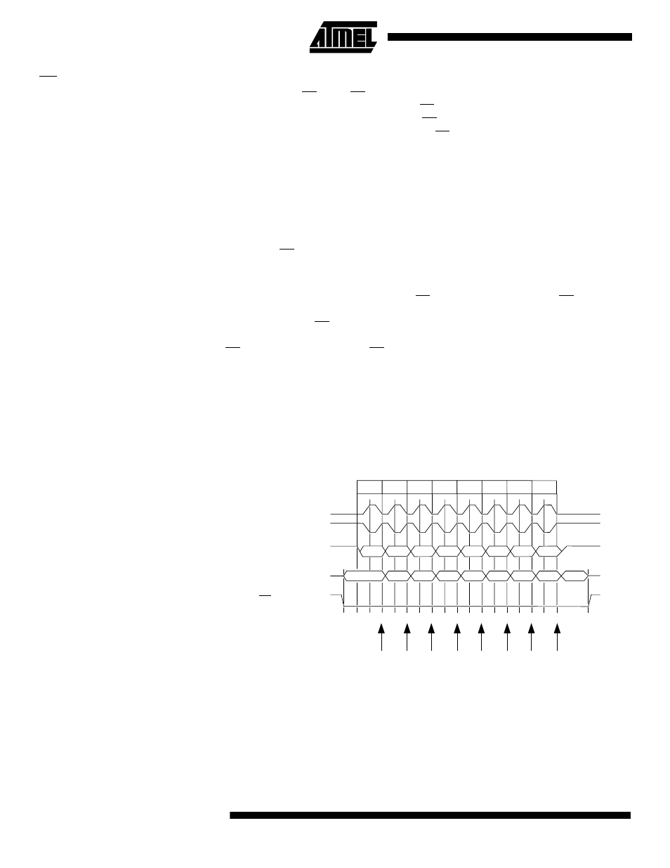
There are four combinations of SCK phase and polarity with respect to serial data,
which are determined by control bits CPHA and CPOL. The SPI data transfer formats
are shown in Figure 39 and Figure 40.
Figure 39. SPI Transfer Format with CPHA = 0 and DORD = 0
SAMPLE
*Not defined but normally MSB of character just received.
SCK CYCLE#
(FOR REFERENCE)
SCK (CPOL=0)
SCK (CPOL=1)
MOSI
(FROM MASTER)
MISO
(FROM SLAVE)
SS (TO SLAVE)
1
2
3
4
5
6
7
8
MSB
1
2
3
4
5
6
LSB
MSB
1
2
3
4
5
6
LSB
*
