Rainbow Electronics AT90LS8535 User Manual
Page 55

55
AT90S/LS8535
1041H–11/01
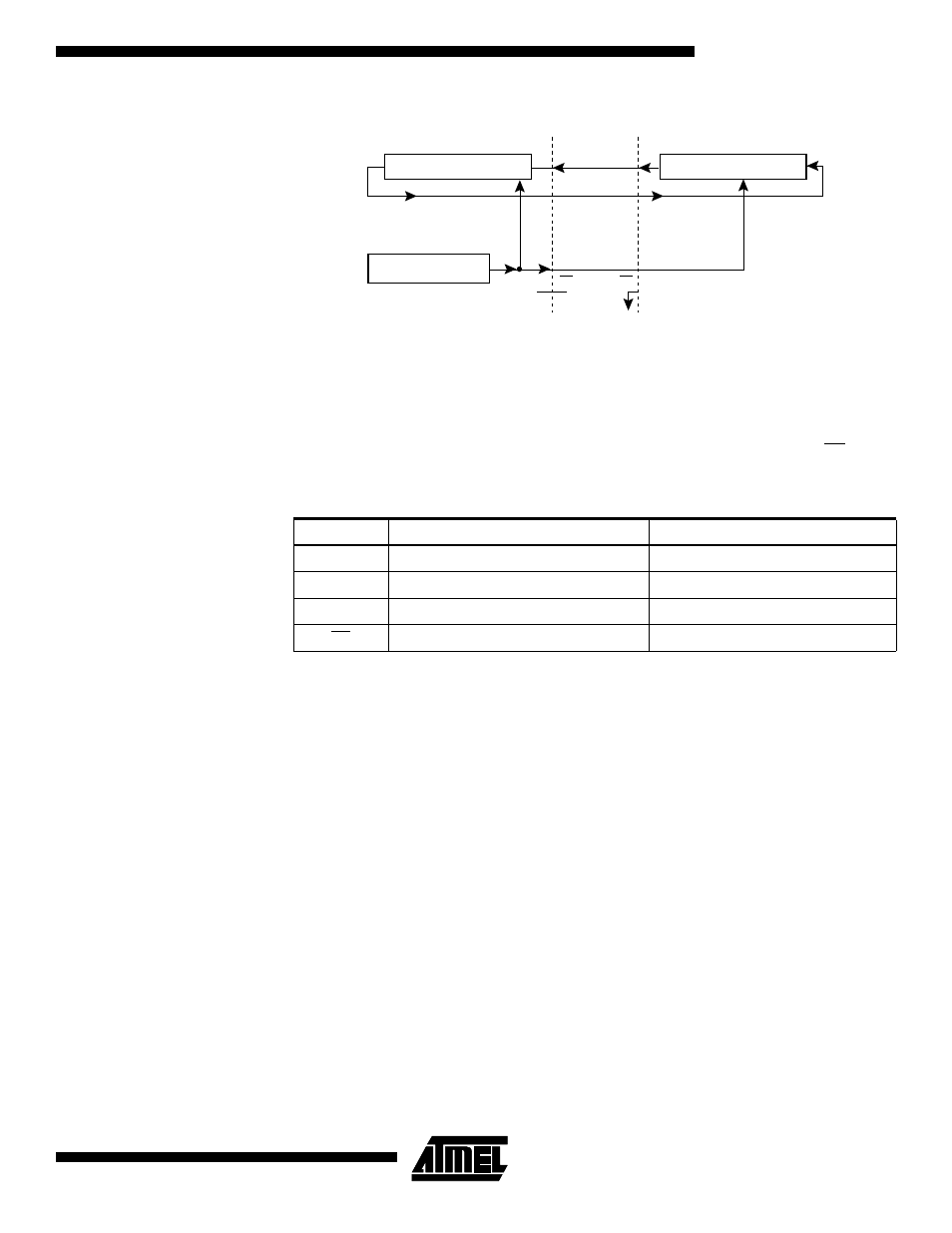
Figure 38. SPI Master-slave Interconnection
The system is single-buffered in the transmit direction and double-buffered in the
receive direction. This means that bytes to be transmitted cannot be written to the SPI
Data Register before the entire shift cycle is completed. When receiving data, however,
a received byte must be read from the SPI Data Register before the next byte has been
completely shifted in. Otherwise, the first byte is lost.
When the SPI is enabled, the data direction of the MOSI, MISO, SCK and SS pins is
overridden according to Table 22.
Note:
See “Alternate Functions of Port B” on page 79 f
or a detailed description of how to
define the direction of the user-defined SPI pins.
Table 22. SPI Pin Overrides
Pin
Direction, Master SPI
Direction, Slave SPI
MOSI
User Defined
Input
MISO
Input
User Defined
SCK
User Defined
Input
SS
User Defined
Input
MSB
MASTER
LSB
8 BIT SHIFT REGISTER
MSB
MASTER
LSB
8 BIT SHIFT REGISTER
MISO
MOSI
SPI
CLOCK GENERATOR
SCK
SS
MISO
MOSI
SCK
SS
V
CC
