Timer/counter0 control register – tccr0, Timer counter 0 – tcnt0 – Rainbow Electronics AT90LS8535 User Manual
Page 34
34
AT90S/LS8535
1041H–11/01
Timer/Counter0 Control
Register – TCCR0
• Bits 7..3 – Res: Reserved Bits
These bits are reserved bits in the AT90S8535 and always read zero.
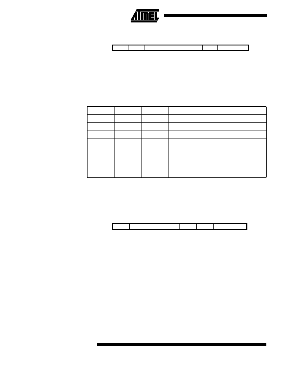
• Bits 2, 1, 0 – CS02, CS01, CS00: Clock Select0, Bits 2, 1 and 0
The Clock Select0 bits 2,1 and 0 define the prescaling source of Timer/Counter0.
The Stop condition provides a Timer Enable/Disable function. The prescaled CK modes
are scaled directly from the CK oscillator clock. If the external pin modes are used, the
corresponding setup must be performed in the actual Data Direction Control Register
(cleared to zero gives an input pin).
Timer Counter 0 – TCNT0
The Timer/Counter0 is realized as an up-counter with read and write access. If the
Timer/Counter0 is written and a clock source is present, the Timer/Counter0 continues
counting in the clock cycle following the write operation.
Bit
7
6
5
4
3
2
1
0
$33 ($53)
–
–
–
–
–
CS02
CS01
CS00
TCCR0
Read/Write
R
R
R
R
R
R/W
R/W
R/W
Initial Value
0
0
0
0
0
0
0
0
Table 10. Clock 0 Prescale Select
CS02
CS01
CS00
Description
0
0
0
Stop, Timer/Counter0 is stopped.
0
0
1
CK
0
1
0
CK/8
0
1
1
CK/64
1
0
0
CK/256
1
0
1
CK/1024
1
1
0
External Pin T0, falling edge
1
1
1
External Pin T0, rising edge
Bit
7
6
5
4
3
2
1
0
$32 ($52)
MSB
LSB
TCNT0
Read/Write
R/W
R/W
R/W
R/W
R/W
R/W
R/W
R/W
Initial Value
0
0
0
0
0
0
0
0