Eeprom read/write access, Eeprom address register – eearh and eearl, Eeprom data register – eedr – Rainbow Electronics AT90LS8535 User Manual
Page 51: Eeprom control register – eecr
51
AT90S/LS8535
1041H–11/01
EEPROM Read/Write
Access
The EEPROM access registers are accessible in the I/O space.
The write access time is in the range of 2.5 - 4 ms, depending on the V
CC
voltages. A
self-timing function lets the user software detect when the next byte can be written. A
special EEPROM Ready interrupt can be set to trigger when the EEPROM is ready to
accept new data.
In order to prevent unintentional EEPROM writes, a specific write procedure must be fol-
lowed. Refer to the description of the EEPROM Control Register for details on this.
When the EEPROM is read, the CPU is halted for four clock cycles before the next
instruction is executed. When the EEPROM is written, the CPU is halted for two clock
cycles before the next instruction is executed.
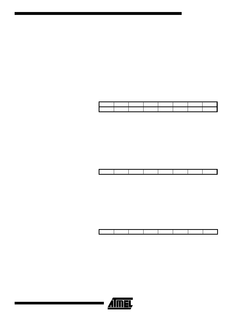
EEPROM Address Register –
EEARH and EEARL
The EEPROM address registers (EEARH and EEARL) specify the EEPROM address in
the 512-byte EEPROM space. The EEPROM data bytes are addressed linearly
between 0 and 511.
EEPROM Data Register –
EEDR
• Bits 7..0 – EEDR7.0: EEPROM Data
For the EEPROM write operation, the EEDR register contains the data to be written to
the EEPROM in the address given by the EEAR register. For the EEPROM read opera-
tion, the EEDR contains the data read out from the EEPROM at the address given by
EEAR.
EEPROM Control Register –
EECR
• Bit 7..4 – Res: Reserved Bits
These bits are reserved bits in the AT90S8535 and will always read as zero.
• Bit 3 – EERIE: EEPROM Ready Interrupt Enable
When the I-bit in SREG and EERIE are set (one), the EEPROM Ready Interrupt is
enabled. When cleared (zero), the interrupt is disabled. The EEPROM Ready Interrupt
generates a constant interrupt when EEWE is cleared (zero).
Bit
15
14
13
12
11
10
9
8
$1F ($3F)
–
–
–
–
–
–
–
EEAR8
EEARH
$1E ($3E)
EEAR7
EEAR6
EEAR5
EEAR4
EEAR3
EEAR2
EEAR1
EEAR0
EEARL
7
6
5
4
3
2
1
0
Read/Write
R
R
R
R
R
R
R
R/W
R/W
R/W
R/W
R/W
R/W
R/W
R/W
R/W
Initial Value
0
0
0
0
0
0
0
X
X
X
X
X
X
X
X
X
Bit
7
6
5
4
3
2
1
0
$1D ($3D)
MSB
LSB
EEDR
Read/Write
R/W
R/W
R/W
R/W
R/W
R/W
R/W
R/W
Initial Value
0
0
0
0
0
0
0
0
Bit
7
6
5
4
3
2
1
0
$1C ($3C)
–
–
–
–
EERIE
EEMWE
EEWE
EERE
EECR
Read/Write
R
R
R
R
R/W
R/W
R/W
R/W
Initial Value
0
0
0
0
0
0
0
0