Figure 19. crystal placement on pcb – Rainbow Electronics DS2422 User Manual
Page 43
DS2422
43 of 48
and decides whether to continue with an operation or to reread the portion of the data with the CRC error. With the
initial pass through the Read Memory with CRC flow chart, the 16-bit CRC value is the result of shifting the
command byte into the cleared CRC generator, followed by the 2 address bytes and the data bytes. The password
is excluded from the CRC calculation. Subsequent passes through the Read Memory with CRC flow chart will
generate a 16-bit CRC that is the result of clearing the CRC generator and then shifting in the data bytes
.
With the Write Scratchpad command the CRC is generated by first clearing the CRC generator and then shifting in
the command code, the Target Addresses TA1 and TA2 and all the data bytes. The DS2422 will transmit this CRC
only if the data bytes written to the scratchpad include scratchpad ending offset 11111b. The data may start at any
location within the scratchpad.
With the Read Scratchpad command the CRC is generated by first clearing the CRC generator and then shifting in
the command code, the Target Addresses TA1 and TA2, the E/S byte, and the scratchpad data starting at the
target address. The DS2422 will transmit this CRC only if the reading continues through the end of the scratchpad,
regardless of the actual ending offset. For more information on generating CRC values see Application Note 27.
Figure 18. CRC-16 Hardware Description and Polynomial
Polynomial = X
16
+ X
15
+ X
2
+ 1
X
0
X
1
X
2
X
3
X
4
X
5
X
6
X
7
X
8
X
9
X
10
X
11
X
12
X
13
X
14
X
15
X
16
1
st
STAGE
2
nd
STAGE
3
rd
STAGE
4
th
STAGE
6
th
STAGE
5
th
STAGE
7
th
STAGE
8
th
STAGE
9
th
STAGE
10
th
STAGE
11
th
STAGE
12
th
STAGE
13
th
STAGE
14
th
STAGE
15
th
STAGE
16
th
STAGE
INPUT DATA
CRC
OUTPUT
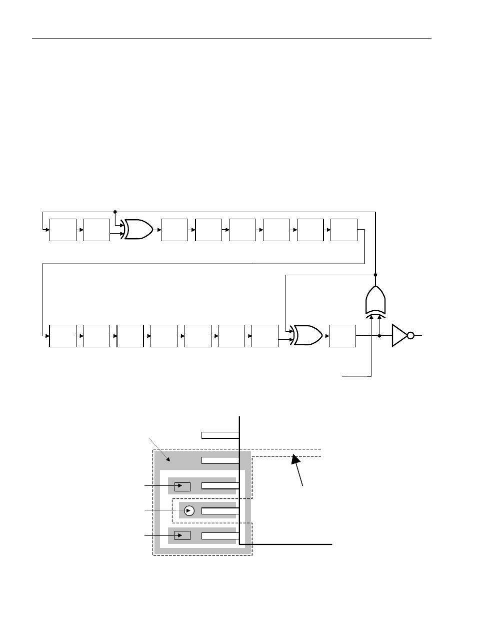
Figure 19. Crystal Placement on PCB
Local ground
plane beneath
signal plane or on
other side of pcb
Guard ring on
signal plane
Crystal
Pad
Crystal
Pad
VIA
AGND
X1
ALARM
X2