Rainbow Electronics DS2422 User Manual
Page 11
DS2422
11 of 48
MEMORY
The memory map of the DS2422 is shown in Figure 7. The 512 bytes general-purpose SRAM are located in pages
0 through 15. The various registers to set up and control the device fill page 16 and 17, called Register Pages 1
and 2 (details in Figure 8). Pages 18 and 19 provide storage space for calibration data. They can alternatively be
used as extension of the general-purpose memory. The Trim Register Page holds registers that are used to tune
the timing of the serial data interface and to trim the on-chip temperature converter. The "datalog" logging memory
starts at address 1000h (page 128) and extends over 256 pages. The memory pages 20 to 31 and 33 to 127
are
reserved for future extensions. The scratchpad is an additional page that acts as a buffer when writing to the SRAM
memory or the register page. The data- and calibration memory can be written at any time. The access type for the
two register pages and the Trim Register Page is register-specific and depends on whether the device is pro-
grammed for a mission. Figures 8A and 8B show
the details. The datalog memory is read-only for the user. It is
written solely under supervision of the on-chip control logic. Due to the special behavior of the write access logic
(write scratchpad, copy scratchpad) it is recommended to only write full pages at a time. This also applies to all the
register pages and the calibration memory. See section Address Register and Transfer Status for details.
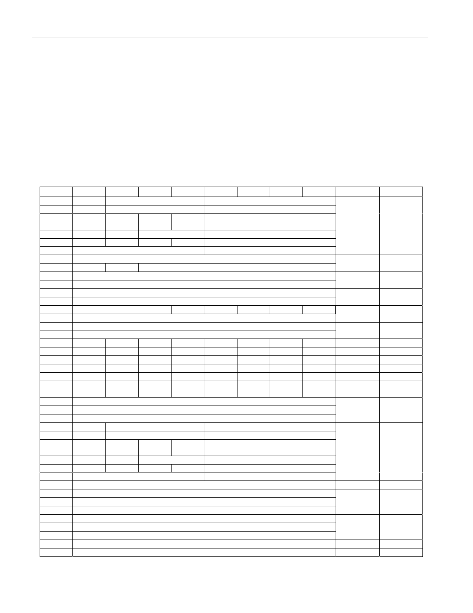
Figure 8A. DS2422 Register Pages Map
ADDR
b7
b6
b5
b4
b3
b2
b1
b0
Function
Access*
0200h
0
10 Seconds
Single Seconds
0201h
0
10 Minutes
Single Minutes
Real-
0202h
0
12/24
20h.
AM/PM
10h.
Single Hours
Time Clock
R/W; R
0203h
0
0
10 Date
Single Date
Registers
0204h
CENT
0
0
10m.
Single Months
0205h
10 Years
Single Years
0206h
Low Byte
Sample
0207h
0
0
High Byte
Rate
R/W; R
0208h
Low Threshold
Temp.
0209h
High Threshold
Alarms
R/W; R
020Ah
Low Threshold
020Bh
High Threshold
Data
Alarms
R/W; R
020Ch
Low Byte
0
0
0
0
0
Latest
R; R
020Dh
High Byte
Temp.
020Eh
Low Byte
020Fh
High Byte
Latest
Data
R; R
0210h
0
0
0
0
0
0
ETHA
ETLA
T.Alm.En.
R/W; R
0211h
1
1
1
1
1
1
EDHA
EDLA
D.Alm.En.
R/W; R
0212h
0
0
0
0
0
0
EHSS
EOSC
RTC En.
R/W; R
0213h
1
1
SUTA
RO
DLFS
TLFS
EDL
ETL
Mis. Cntrl.
R/W; R
0214h
BOR
1
1
1
DHF
DLF
THF
TLF
Alm. Stat.
R; R
0215h
1
1
0
WFTA
MEMC
LR
0
MIP
0
Gen. Stat.
R; R
0216h
Low Byte
Start
0217h
Center Byte
Delay
R/W; R
0218h
High Byte
Counter
0219h
0
10 Seconds
Single Seconds
021Ah
0
10 Minutes
Single Minutes
021Bh
0
12/24
20h.
AM/PM
10h.
Single Hours
Mission
Time
R; R
021Ch
0
0
10 Date
Single Date
Stamp
021Dh
CENT
0
0
10m.
Single Months
021Eh
10 Years
Single Years
021Fh
(no function; reads 00h)
(N/A)
R; R
0220h
Low Byte
Mission
0221h
Center Byte
Samples
R; R
0222h
High Byte
Counter
0223h
Low Byte
Device
0224h
Center Byte
Samples
R; R
0225h
High Byte
Counter
0226h
Configuration Code
Flavor
R; R
0227h
EPW
PW. Cntrl.
R/W; R