Rainbow Electronics DS2422 User Manual
Page 4
DS2422
4 of 48
Note 1:
System Requirement
Note 2:
Maximum allowable pullup resistance is a function of the number of 1-Wire devices in the system and 1-Wire recovery times. The
specified value here applies to systems with only one device and with the minimum 1-Wire recovery times. For more heavily
loaded systems, an active pullup such as that found in the DS2480B may be required.
Note 3:
Capacitance on the data pin could be 800pF when V
PUP
is first applied. If a 2.2k
W resistor is used to pull up the data line, 2.5µs
after V
PUP
has been applied the parasite capacitance will not affect normal communications.
Note 4:
Guaranteed by design, not production tested.
Note 5:
V
TL
, V
TH
are a function of the internal supply voltage.
Note 6:
Voltage below which, during a falling edge on I/O, a logic '0' is detected.
Note 7:
The voltage on I/O needs to be less or equal to V
ILMAX
whenever the master drives the line low.
Note 8:
Voltage above which, during a rising edge on I/O, a logic '1' is detected.
Note 9:
After V
TH
is crossed during a rising edge on I/O, the voltage on I/O has to drop by V
HY
to be detected as logic '0'.
Note 10:
The I-V characteristic is linear for voltages less than 1V.
Note 11:
The earliest recognition of a negative edge is possible at t
REH
after V
TH
has been previously reached.
Note 12:
Highlighted numbers are NOT in compliance with the published iButton standards. See comparison table below.
Note 13:
Interval during the negative edge on I/O at the beginning of a Presence Detect pulse between the time at which the voltage is
90% of V
PUP
and the time at which the voltage is 10% of V
PUP
.
Note 14:
e represents the time required for the pullup circuitry to pull the voltage on I/O up from V
IL
to V
TH
.
Note 15:
d represents the time required for the pullup circuitry to pull the voltage on I/O up from V
IL
to the input high threshold of the bus
master.
Note 16:
This is the expected range when using a crystal equivalent to the KDS SN14J (12.5pF).
Note 17:
Time to reach 63% of the temperature change; measured at a temperature transition step from +25°C to +85°C.
Note 18:
A 2-point calibration trim at 3V must be done to achieve the specified accuracy at 3V. An application note is available to help
developers perform the calibration by writing the trim registers to properly orient the error curve.
Note 19:
The duration is user-programmable from 0ms (code 00h) to 127.5ms (code FFh) with a tolerance of ±0.5ms. See Delay Register,
address 400h, for details.
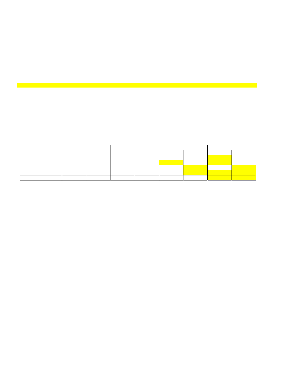
STANDARD VALUES
DS2422 VALUES
PARAMETER
STANDARD SPEED
OVERDRIVE SPEED
STANDARD SPEED
OVERDRIVE SPEED
NAME
MIN
MAX
MIN
MAX
MIN
MAX
MIN
MAX
t
SLOT
(incl. t
REC
)
61µs
(undef.)
7µs
(undef.)
65µs
1)
(undef.)
9.5µs
(undef.)
t
RSTL
480µs
(undef.)
48µs
80µs
690µs
720µs
70µs
80µs
t
PDH
15µs
60µs
2µs
6µs
15µs
63.5µs
2µs
7µs
t
PDL
60µs
240µs
8µs
24µs
60µs
287µs
7µs
28µs
t
W0L
60µs
120µs
6µs
16µs
60µs
120µs
7.5µs
12µs
1)
Intentional change, longer recovery time requirement due to modified 1-Wire front end.