56 mhz type b rf reader – Rainbow Electronics AT88RF1354 User Manual
Page 39
13.56 MHz Type B RF Reader
39
8547A
−RFID−10/08
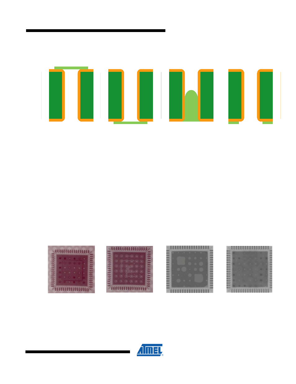
Figure D-4. Solder Mask Options for Thermal Vias
Via Tenting
from Top
Via Tenting
from Bottom
Via Plugging
from Bottom
Via Encroached
from Bottom
All of these options have pros and cons when mounting the QFN package on the board. While via tenting from the
top side may result in smaller voids, the presence of the solder mask on the top side of the board may hinder proper
paste printing. On the other hand, both via tenting from bottom or via plugging from bottom may result in larger voids
due to out-gassing covering more than two vias. Finally, encroached vias allow the solder to wick inside the vias and
reduce the size of the voids. However, it also results in lower standoff of the package, which is controlled by the
solder underneath the exposed pad. Figure D-5. shows representative x-rays of QFN packages mounted on the
boards with the different via treatments.
Encroached via, depending on the board thickness and the amount of solder printed underneath the exposed pad,
may also result in solder protruding from the other side of the board. Note that the vias are not completely filled with
solder, suggesting that solder wets down the via walls until the ends are plugged. This protrusion is a function of the
PCB thickness, the amount of paste coverage in the thermal pad region, and the surface finish of the PCB. Atmel’s
experience is that this protrusion can be avoided by using a lower volume of the solder paste and reduced reflow
peak temperature. If solder protrusion cannot be avoided, the QFN components may have to be assembled on the
top side (or final pass) assembly, as the protruded solder will impede acceptable solder paste printing on the other
side of the PCB.
Figure D-5. X-ray showing Voids in Thermal Pad Solder Joint
Vias Tented
from Top
Vias Tented
from Bottom
Via Plugged
from Bottom
Via Encroached
from Bottom