Rainbow Electronics MAX6963 User Manual
Page 19
Invert Pixels (Bit D1)
The invert pixels (IP) bit in the global panel configura-
tion register controls whether the display memory is
used directly or inverted (Table 17).
Current Plane Identification (Bits D2, D3)
The current plane bits in the global panel configuration
register identify which memory plane is currently being
used to control the display panel (Table 18). These bits
are read only; written data is ignored.
Ripple Sync (Bit D4)
The ripple sync feature, when enabled in the global
panel configuration register, desynchronizes the multi-
plex timing of all the interconnected MAX6960 drivers
on a display panel by OSC/4 (Table 19). This delay
spreads the drive transitions among the drivers to
spread power-supply peak-current demand, and ease
decoupling. The maximum delay from first driver to last
driver is 244µs with the maximum of 256 drivers used.
This is too short a time to cause visible artifacts.
Mux Flip (Bit D5)
The mux flip feature in the global panel configuration
register reverses the panel PWM timing for alternate
drivers when enabled (Table 20). Again, this spreads
power-supply peak-current demand.
Color Control (Bit D6)
The color control bit in the global panel configuration
register selects whether a monocolor or RGY display
panel is built. Select monocolor when building an RGB
panel as shown in Figure 17. This bit is fixed at zero for
the MAX6962 and MAX6963, and a write to this bit is
ignored for these parts.
Planes/Intensity Control (Bit D7)
The planes/intensity (PI) control bit in the global panel
configuration register selects whether the display mem-
ory is configured as four planes with 1-bit-per pixel per
color-intensity control, or two planes with 2-bits-per
pixel per color-intensity control. This bit is fixed at zero
for the MAX6961 and MAX6963, and a write to this bit is
ignored for these parts.
Pixel Intensity Scale Register
The pixel intensity scale register (Table 24) sets the
graduation type used when 2-bits-per-pixel intensity
control is selected by setting the PI bit (Table 22). The
pixel level-intensity control can be set to be either
MAX6960–MAX6963
4-Wire Serially Interfaced
8 x 8 Matrix Graphic LED Drivers
______________________________________________________________________________________
19
REGISTER DATA
REGISTER
ADDRESS
CODE (HEX)
D7
D6
D5
D4
D3
D2
D1
D0
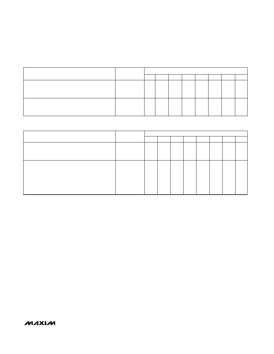
Ripple sync is disabled; all interconnected
MAX6960s on the same 4-wire bus resynchronize
together.
0x0D
PI
C
F
0
DP1
DP0
IP
S
Ripple sync is enabled; all interconnected
MAX6960s on the same 4-wire bus resynchronize
with a 0.9537µs delay between adjacent devices.
0x0D
PI
C
F
1
DP1
DP0
IP
S
Table 19. Global Panel Configuration—Ripple Sync Control (R Data Bit D4) Format
REGISTER DATA
REGISTER
ADDRESS
CODE (HEX)
D7
D6
D5
D4
D3
D2
D1
D0
Mux flip is disabled: all interconnected MAX6960s
on the same 3-wire bus resynchronize to the
multiplex timing shown in Figure 11.
0x0D
PI
C
0
R
DP1
DP0
IP
S
Mux flip is enabled: all interconnected MAX6960s on
the same 3-wire bus resynchronize with MAX6960s
with even driver addresses (0, 2, 4 to 254) operating
to the multiplex timing shown in Figure 11, and
MAX6960s with odd driver addresses (1, 3, 5 to 255)
operating to the flipped multiplex timing shown in
Figure 12.
0x0D
PI
C
1
R
DP1
DP0
IP
S
Table 20. Global Panel Configuration—Mux Flip Control (F Data Bit D5) Format