Table 5. frame modulation with pixel intensity, Table 6. panel configuration – Rainbow Electronics MAX6963 User Manual
Page 10
MAX6960–MAX6963
4-Wire Serially Interfaced
8 x 8 Matrix Graphic LED Drivers
10
______________________________________________________________________________________
green.The MAX6960 uses display memory planes to
store the display images. A memory plane is the exact
amount of memory required to store the display image.
The memory plane architecture allows one plane to be
used to refresh the display, while at least one other plane
is available to build up the next image. The global plane
counter register (Table 30) allows the plane used to
refresh the display to be selected either directly on com-
mand, or automatically under MAX6960 control.
Automatic plane switching can be set from 63 plane
changes a second to one plane change every 63s.
Display Memory Addressing
The MAX6960 contains 64 bytes of display mapping
memory. This display memory provides four memory
planes (of 16 bytes) when 1-bit-per-pixel intensity con-
trol is selected, or two memory planes (of 32 bytes)
when 2-bits-per-pixel intensity control is used (Table 6).
The 64 bytes of display memory in a MAX6960 could
be accessed with 6 bits of addressing on a driver-by-
driver basis.
The MAX6960 uses a 14-bit addressing scheme. The
address map encompasses up to 256 MAX6960 dri-
vers, all connected to the host through a common 4-
wire interface, and also interconnected through a local
3-wire interface. The purpose of the 3-wire interface is
to actively segment the 14-bit address space among
the (up to) 256 MAX6960s.
The total display memory is already partitioned among
these MAX6960 drivers in a register format. The
MAX6960s repartition these registers to appear as con-
tiguous planes of display memory, organized by color
(red, then green) and then into planes (P0 to P4)
(Table 6).
Register Addressing Modes
The MAX6960 accepts 8-bit, 16-bit, and 24-bit trans-
missions. All MAX6960s sharing an interface receive
and decode all these transmissions, but the content of
a transmission determines which MAX6960s store and
use a particular transmission, and which discard it
(Table 7).
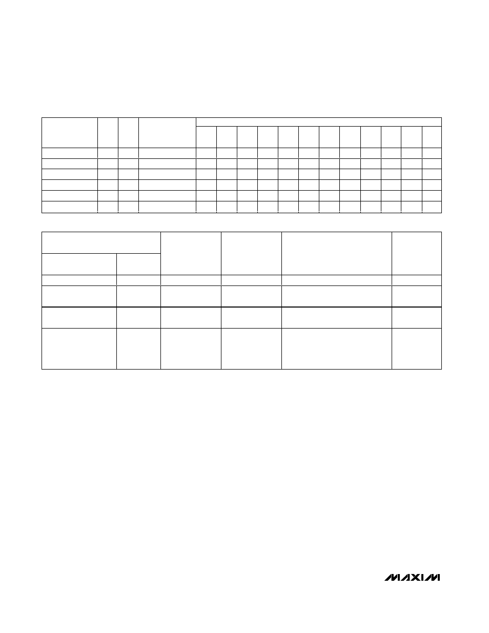
PATTERN OF MULTIPLEX CYCLES FOR WHICH A PIXEL IS ENABLED
PIXEL
GRADUATION
BIT
BIT
PIXEL
INTENSITY
SETTING
0
1
2
3
4
5
6
7
8
9
10
11
Both
1
1
Full
1
1
1
1
1
1
1
1
1
1
1
1
Arithmetic
1
0
2/3
1
0
1
1
0
1
1
0
1
1
0
1
Geometric
1
0
1/2
1
0
1
0
1
0
1
0
1
0
1
0
Arithmetic
0
1
1/3
0
1
0
0
1
0
0
1
0
0
1
0
Geometric
0
1
1/4
0
1
0
0
0
1
0
0
0
1
0
0
Both
0
0
Off
0
0
0
0
0
0
0
0
0
0
0
0
Table 5. Frame Modulation with Pixel Intensity
GLOBAL PANEL CONFIGURATION
REGISTER
PLANES/INTENSITY
(PI BIT)
COLOR
(C BIT)
PIXEL-LEVEL
INTENSITY
CONTROL
DISPLAY TYPE
DISPLAY MAPPING
ADDRESSES PER PLANE
DISPLAY
PLANES
AVAILABLE
0
0
1 bit per pixel
Monocolor
16 red contiguous
4
0
1
1 bit per pixel
RGY
8 red contiguous,
8 green contiguous
4
1
0
2 bits per pixel
Monocolor
16 red contiguous,
16 red contiguous
2
1
1
2 bits per pixel
RGY
16 red
(2 noncontiguous groups of 8),
16 green
(2 noncontiguous groups of 8)
2
Table 6. Panel Configuration