Rainbow Electronics MAX6963 User Manual
Page 18
MAX6960–MAX6963
The global driver devices register should be written
with the total number of MAX6960s interconnected on
the 3-wire interface, minus 1 (Table 13). For the four
panel examples shown in Figures 1 and 2, 24
MAX6960s are used, so the global driver devices regis-
ter should be written with the value 23, or 0x17.
The global driver rows register should be written with
the number of MAX6960s per panel row, minus 1
(Table 14). For the panel examples shown in Figure 1
and Figure 2, there are six MAX6960s per row, so the
global driver rows register should be written with the
value 5.
The values stored in the global driver devices register
and the global driver rows register, together with the C
and Pl bits in the global panel configuration register
(Tables 21 and 22), are used by the 3-wire interface
configuration engine to reconfigure display memory
addressing among the interconnected MAX6960s.
Global Panel Configuration Register
The configuration register contains eight device set-
tings (Table 15 to Table 22).
Shutdown Mode (Bit D0)
Shutdown mode is exited by clearing the S bit in the
global panel configuration register (Table 16). When
the MAX6960 is in shutdown mode, LED driver outputs
ROW1–ROW8 and COL1–COL16 are tri-stated, and
multiplexing is halted. Data in the configuration regis-
ters remains unaltered. For minimum supply current in
shutdown mode, logic inputs should be at GND or V+
potential. Shutdown mode is exited by setting the S bit
in the global panel configuration register.
4-Wire Serially Interfaced
8 x 8 Matrix Graphic LED Drivers
18
______________________________________________________________________________________
REGISTER DATA
REGISTER
ADDRESS
CODE (HEX)
D7
D6
D5
D4
D3
D2
D1
D0
Global panel configuration register
0x0D
PI
C
F
R
DP1
DP0
IP
S
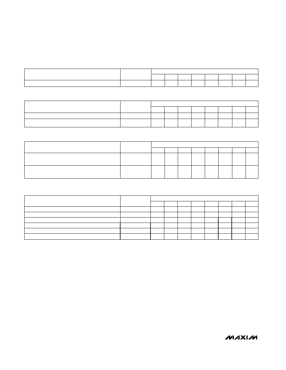
Table 15. Global Panel Configuration Register Format
Table 16. Global Panel Configuration—Shutdown Control (S Data Bit D0) Format
REGISTER DATA
REGISTER
ADDRESS
CODE (HEX)
D7
D6
D5
D4
D3
D2
D1
D0
Logic 1 in display memory lights the appropriate
LED (normal logic)
0x0D
PI
C
F
R
DP1
DP0
0
S
Logic 0 in display memory lights the appropriate
LED (invert logic)
0x0D
PI
C
F
R
DP1
DP0
1
S
Table 17. Global Panel Configuration—Invert Pixels (IP Data Bit D1) Format
REGISTER DATA
REGISTER
ADDRESS
CODE (HEX)
D7
D6
D5
D4
D3
D2
D1
D0
Current display plane is P0
0x0D
PI
C
F
R
0
0
IP
S
Current display plane is P1
0x0D
PI
C
F
R
0
1
IP
S
Current display plane is P2
0x0D
0
C
F
R
1
0
IP
S
Current display plane is P0
0x0D
1
C
F
R
1
0
IP
S
Current display plane is P3
0x0D
0
C
F
R
1
1
IP
S
Current display plane is P1
0x0D
1
C
F
R
1
1
IP
S
Table 18. Global Panel Configuration—Current Plane (DP0, DP1 Data Bit D2, D3) Format
REGISTER DATA
REGISTER
ADDRESS
CODE (HEX)
D7
D6
D5
D4
D3
D2
D1
D0
Shutdown
0x0D
PI
C
F
R
DP1
DP0
IP
0
Normal operation
0x0D
PI
C
F
R
DP1
DP0
IP
1